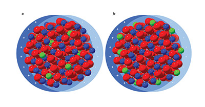
One method of altering the electrical properties of a semiconductor is by introducing impurities called dopants. A team led by Delia Milliron, a chemist in the Molecular Foundry’s Inorganic Nanostructures Facility, has demonstrated that equally important as the amount of dopant is how the dopant is distributed on the surface and throughout the material. This opens the door for engineering the distribution of the dopant in order to control what wavelength the material will absorb and more generally how light interacts with the nanocrystals.
“Doping in semiconductor nanocrystals is still an evolving art,” says Milliron. “Only in the last few years have people begun to observe interesting optical properties as a result of introducing dopants to these materials, but how the dopants are distributed within the nanocrystals remains largely unknown. What sites they occupy and where they are situated throughout the material greatly influences optical properties.”
Milliron’s most recent claim to fame, a “smart window” technology that not only blocks natural infrared (IR) radiation while allowing the passage of visible light through transparent coated glass, but also allows for independent control over both kinds of radiation, relies on a doped semiconductor called indium tin oxide (ITO).

