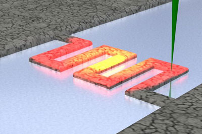
A team of researchers working at the Foundry have created a thermal imaging technique that can “see” how temperature changes from point to point inside the smallest electronic circuits.
The technique, called plasmon energy expansion thermometry, or PEET, allows temperatures to be mapped at the nanometer scale using a transmission electron microscope. This shatters the previous record for thermal imaging resolution and could eventually lead to faster and more capable electronics.
PEET focuses a microscope’s electron beam to a point and measures energy changes that are related to the creation of plasmon waves. Since this energy loss is sensitive to a material’s density, and density is related to a material’s temperature, the team was able to map temperature with nanometer-scale spatial resolution.

