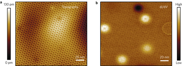
Observing individual nanoscale defects in bulk insulators, a ubiquitous and essential component to almost all devices, has remained elusive: it’s far easier to image the detailed electrical structure of conductors than insulators. Now, researchers at Berkeley Lab using the Molecular Foundry have demonstrated a new method that can be applied to study individual defects in a widely used bulk insulating material, hexagonal boron nitride (h-BN), by employing scanning tunneling microscopy (STM).
Normally, STM is used to study conductors and cannot be used to study bulk insulators, since electrical current does not typically flow through an insulator. The team overcame this obstacle by capping the h-BN with a single sheet of graphene that was synthesized and characterized at the Molecular Foundry. This approach allowed researchers to visualize the charged defects embedded in the underlying BN crystal. In other words, graphene was used as a window to look into the insulator.

