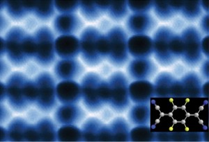
In what could prove to be a significant advance in the fabrication of graphene-based nanodevices, a team of Molecular Foundry users has discovered a new mechanism for assembling two-dimensional (2D) molecular “islands” that could be used to modify graphene at the nanometer scale.
Graphene is a sheet of pure carbon just one atom thick through which electrons speed 100 times faster than they move through silicon. Graphene is also slimmer and stronger than silicon, making it a potential superstar material for the electronics industry.
The 2D islands could be used to control the charge-carrier density in graphene substrates, as well as to modify how electrons move through graphene-based devices. They might also be used to form precise nanoscale patterns that exhibit atomic-scale structural perfection unmatched by conventional fabrication techniques.

