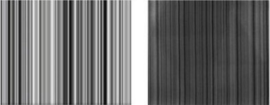
Through a collaboration with two Berkeley Lab user facilities – the Molecular Foundry and ALS – as well as two other national labs, a small Bay Area company has made big news in the semiconductor world. Modern electronics are getting smaller and smaller, which means the demands on semiconductor manufacturers are increasing. To ensure the quality and consistency of substrates, wafer manufacturers employ metrology tools to control the quality of their materials, but those tools are not as precise as the industry needs. Last year, Hayward-based aBeam Technologies made history with the development of the finest metrology tool in the world, utilizing a fabricated pattern with line widths down to 1.5 nanometers. The collaborative effort earned them a 2015 R&D100 Award.
aBeam has a long history of collaboration with the Molecular Foundry, relying on state-of-the-art nanofabrication equipment and utilizing the expertise and advice of the Molecular Foundry’s Nanofabrication Facility staff.

