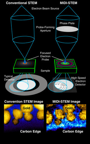
Electrons can extend our view of microscopic objects well beyond what’s possible with visible light, all the way to the atomic scale. A popular method in electron microscopy for looking at tough, resilient materials in atomic detail is called STEM, or scanning transmission electron microscopy, but the highly focused beam of electrons used in STEM can also easily destroy delicate samples.
To address this challenge, a team of scientists at the Molecular Foundry have developed a new imaging technique, tested on samples of nanoscale gold and carbon, that greatly improves images of light elements using fewer electrons. The team was brought together through the Foundry’s new Theme Postdoc program that is designed to tackle highly multidisciplinary research challenges that would result in the development of new capabilities for future users.
The newly demonstrated technique, dubbed MIDI-STEM, for matched illumination and detector interferometry scanning transmission electron microscopy (STEM), combines STEM with an optical device called a phase plate that modifies the alternating peak-to-trough, wave-like properties (called the phase) of the electron beam. This phase plate modifies the electron beam in a way that allows subtle changes in a material to be measured, even revealing materials that would be invisible in traditional STEM imaging.
“The MIDI-STEM method provides hope for seeing structures with a mixture of heavy and light elements, even when they are bunched closely together,” said Colin Ophus, a project scientist at the Molecular Foundry and lead author of a study.

