Next-generation solar cells made of super-thin films of semiconducting material hold promise because they’re relatively inexpensive and flexible enough to be applied just about anywhere.
Researchers are working to dramatically increase the efficiency at which thin-film solar cells convert sunlight to electricity. But it’s a tough challenge, partly because a solar cell’s subsurface realm—where much of the energy-conversion action happens—is inaccessible to real-time, nondestructive imaging. It’s difficult to improve processes you can’t see.
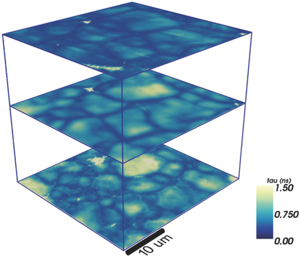
Now, scientists from the Molecular Foundry have developed a way to use optical microscopy to map thin-film solar cells in 3-D as they absorb photons.
The method images optoelectronic dynamics in materials at the micron scale, or much thinner than the diameter of a human hair. This is small enough to see individual grain boundaries, substrate interfaces, and other internal obstacles that can trap excited electrons and prevent them from reaching an electrode, which saps a solar cell’s efficiency.
So far, scientists have used the technique to better understand why adding a specific chemical to solar cells made of cadmium telluride (CdTe)—the most common thin-film material—improves the solar cells’ performance.
The imaging method was born out of a collaboration between Molecular Foundry scientists and Foundry users from PLANT PV Inc., an Alameda, California-based company. While fabricating new solar cell materials at the Molecular Foundry, the team found that standard optical techniques couldn’t image the inner-workings of the materials, so they developed the new technique to obtain this view. Next, scientists from the National Renewable Energy Laboratory (NREL) came to the Molecular Foundry and used the new method to study CdTe solar cells.
To develop the approach, the scientists modified a technique called two-photon microscopy (which is used by biologists to see inside thick samples such as living tissue) so that it can be applied to bulk semiconductor materials.
The method uses a highly focused laser beam of infrared photons that penetrate inside the photovoltaic material. When two low-energy photons converge at the same pinpoint, there’s enough energy to excite electrons. These electrons can be tracked to see how long they last in their excited state, with long-lifetime electrons appearing as bright spots in microscopy images. In a solar cell, long-lifetime electrons are more likely to reach an electrode.
In addition, the laser beam can be systematically repositioned throughout a test-sized solar cell, creating a 3-D map of a solar cell’s entire optoelectronic dynamics.

