By Clarissa Bhargava

Thermoelectrics are materials that can harness heat differences to generate electricity. That’s a very useful trait – many of our devices and processes generate heat, making them warmer than their environments. With thermoelectrics, any temperature gap presents an opportunity to recover electricity or to power small devices. Even our bodies give off heat; instead of wasting that energy, imagine powering your phone as it sits in your pocket!
The game-changing potential of thermoelectric devices has inspired many attempts to create a range of superhero thermoelectric materials, but scientists keep hitting walls in their search. Candidate materials often require highly complex manufacturing processes to achieve even a lukewarm performance. It has been even more difficult to find a suitable materials system for flexible applications; most high-performing thermoelectric materials are rigid, and so far, proposed flexible options have been plagued by stability issues.
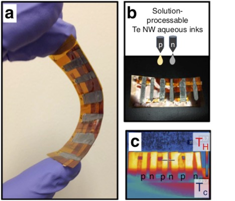
In a breakthrough study led by the Molecular Foundry, scientists have announced a creative new approach to answer these challenges: doped nanowire inks.
The team tackled several problems at once, using nanoscale engineering to make big changes in the material’s properties. First, instead of using a traditional “bulk” material, the researchers crafted tiny nanowires to take advantage of both their high surface areas and their collective flexibility. They were able to make dramatic, controlled changes in the electronic properties of tellurium nanowires by coating the wire surfaces with small molecules. These wires can be printed onto a flexible material like an ink, with regions of different properties patterned like the colors in an inkjet printer.
Electronic devices generally require both n-type and p-type semiconductors, which differ in how charge moves through the material. Engineers can either use distinct materials of each type, or they can alter a single material to have an n-type region and a p-type region. The latter approach is accomplished through ‘doping,’ which usually involves embedding certain atoms into the crystal to change its charge carrier type.
When dealing with thermoelectrics, however, both approaches run into problems. Using two or more materials calls for a complicated and expensive machining process and dashes any chance of making a flexible device. Likewise, changing the carrier type within a single material through traditional doping methods can distort the lattice and interrupt the movement of charge, making it difficult to get the ideal properties for a thermoelectric device.
In a major innovation, the Foundry-led research team changed the electronic properties of tellurium nanowires by crowding their surfaces with small molecules in solution. The high concentration of surface molecules drastically influenced the properties in the wires without interrupting the crystal structure. They were able to change an ordinary p-type material into a strong n-type material, a feat which has never been seen before in tellurium. Free of the drawbacks of using multiple materials or traditional doping, this simple and scalable procedure can be used to build high-quality, flexible thermoelectric devices.
This nano-interface engineering approach has major implications for the future of thermoelectrics and other electronic devices like LEDs. Beyond tellurium, other materials can be fashioned into nanowires and surface-doped to achieve large, controlled changes in their properties. With this option added to engineers’ toolkits, materials that were once dismissed as candidates for a range of applications could come back into play.
Thanks to this research, the new state-of-the-art thermoelectric device may use a material that no one expected, and it may soon be in your pocket, quietly charging your phone.

