Scientific Achievement
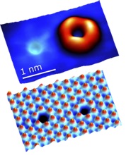
Foundry staff and users have for the first time measured in parallel the exact atomic structure of point defects in 2D materials and their electronic structure by visualizing the associated quantum orbitals using an ultrasharp probe.
Significance and Impact
This is the first time that 2D material properties have been linked to specific defects in the crystal structure. This approach enables systematic defect engineering in 2D materials critical for next generation quantum information science and ”Beyond Moore’s Law” electronic materials.
Research Details
- Researchers used a single carbon monoxide molecule as an ultrasharp “tip” in atomic force microscopy and scanning tunneling microscopy to simultaneously measure the atomic structure of defects and their electronic structure in MoSe2 and WS2.
- Density functional theory and GW calculations were used to model the experiments and to confirm observations.
S. Barja, S.Rafaely-Abramson, B. Schuler, D.Y. Qiu, A. Pulkin, S. Wickenburg, H. Ryu, M.M. Ugeda, C. Kastl, C. Chen, C. Hwang, A. Schwartzberg, S. Aloni, S-K. Mo, D. F. Ogletree, M.F. Crommie, O.V. Yazyev, S.G. Louie, J.B. Neaton, A. Weber-Bargioni. Nat. Commun. 2019 10, 3382. DOI: 10.1038/s41467-019-11342-2
B. Schuler, D.Y. Qiu, S. Rafaely-Abramson, C. Kastl, C. T. Chen, S. Barja, R. J. Koch, F. Ogletree, S. Aloni, A.M Schwartzberg, J.B. Neaton, S. G. Louie, A. Weber-Bargioni. Phys. Rev. Lett. 2019 123, 076801. DOI: 10.1103/PhysRevLett.123.076801
This work has been highlighted by the Department of Energy’s Office of Science.

