By Brooke Kuei

Scientists have been using electrons to probe the structure of materials for decades. In recent years, researchers have manipulated electron beams to become small enough to study materials at the scale of individual atoms – and to pulse fast enough to capture subtle atomic movements.
However, it has been difficult to generate a beam that is both small and fast.
In a collaboration between Berkeley Lab researchers in the Accelerator Technology and Applied Physics Division (ATAP) and the Molecular Foundry, scientists have created a new kind of electron source that has the potential to overcome this hurdle.
The work, which was published Nov. 25, 2019, in Physical Review Applied, demonstrates the potential for a source made from a bullseye plasmonic lens that fires electrons as quickly as existing ultrafast electron beams but with a beam size that is hundreds of times smaller.
“This research is the first part of a more complex and intriguing instrument that I’m thinking about, which will allow us to create ultrafast bursts of electrons emitted from a very small and confined space,” said Daniele Filippetto, a staff scientist at Berkeley Lab’s Accelerator Technology and Applied Physics Division and corresponding author of the study. Such ‘ultrafast’ bursts are quicker than the fastest chemical reaction ever studied.
“This is very limiting, because it means your sample has to look the same over this entire field of view,” said Andrew Minor, director of the National Center for Electron Microscopy, a facility within the Molecular Foundry, and professor at UC Berkeley. “This works well for materials like graphene sheets that look the same everywhere, but we need a much smaller beam to look at things like individual nanowires and nanoparticles.” In materials with multiple components, this large beam size also prevents scientists from looking at the interfaces between different materials.

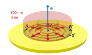
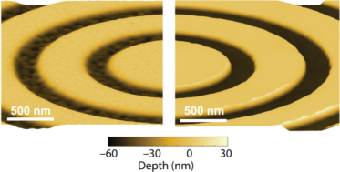
The electron source developed in this study is a gold surface with concentric circular grooves arranged in a bullseye pattern. When a laser hits the gold, the laser transfers energy to surface plasmons – electrons on the surface of the gold that move collectively – and the grooves cause them to ripple inward and outward. When the waves simultaneously hit the center of the bullseye, a small but intense beam of electrons is fired out from the center.
The problem with more conventional ultrafast electron sources is that the size of the beam when it hits the sample is approximately the width of a human hair, which is enormous compared to the nano-scale structures studied at the Molecular Foundry.
“It’s like when you throw a stone into a lake,” explained Filippetto. “You see these waves, but a few seconds after you throw that stone, you see a peak of water coming out where you have interference of the waves.”
The response time of the source is less than 10 femtoseconds (the time it takes for light to travel 3 micrometers), while its size is approximately 100 nanometers (approximately the width of a cell membrane).
For the emitted beam to be as bright as possible, the surface has to be extremely flat. In this case, an atomically flat surface was made using a new nanofabrication technique developed at the Molecular Foundry.
“A couple of years ago, we developed a method to make very smooth surfaces of gold with a peel-off process,” explained Stefano Cabrini, director of the Nanofabrication Facility at the Molecular Foundry. “So we’re able to put a pattern on silicon, deposit the gold onto the silicon, and then peel off the gold. We used this process on the bullseye and it worked.”

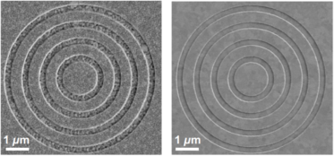
Although the electron source is designed to shoot out electrons when it is hit with light, its ability to do so was tested using the inverse technique: By shining electrons onto the source, the researchers were able to confirm its promising plasmonic behavior by measuring how light came out of it.
The key to the success of this project was the collaboration between different facilities within Berkeley Lab, Filippetto noted.
“Real breakthroughs come when you’re working at the boundaries between different disciplines,” he said. “This project wouldn’t have been possible without the Molecular Foundry. We have a very good collaboration between a group of people who understand each other, and we all put our best efforts forward. We’re seeing the results now.”
The possibility of an ultrafast, tiny electron beam opens up the doors for understanding chemical reactions and structural changes at molecular length scales, particularly for materials that do not look the same over a large area – such as nanoparticles – or for interfaces between different materials.
Moving forward, the team is working on improving the electron source with an improved design. The team also plans to measure electron yield and brightness in a test system, with the final goal of using the source as electron emitter in the HiRES beamline, an ultrafast electron scattering beamline at the Advanced Light Source.
Other directions include designs of nanostructure arrays for emission of large electron currents, exploring the temporal response of the structure to push to sub-femtosecond resolution, and plasmonic-based electron acceleration.
We have a very good collaboration between a group of people who understand each other, and we all put our best efforts forward.
Daniele Filippetto
The Molecular Foundry is a DOE Office of Science User Facility.

