As part of our National Nanotechnology Day celebration, the Molecular Foundry hosted its annual NanoArt image contest to showcase science as art. Entries from Foundry users and staff were voted on by the Foundry community, Berkeley Lab, and the general public.
After nearly 300 votes, the winners have been chosen!
Winning first place:
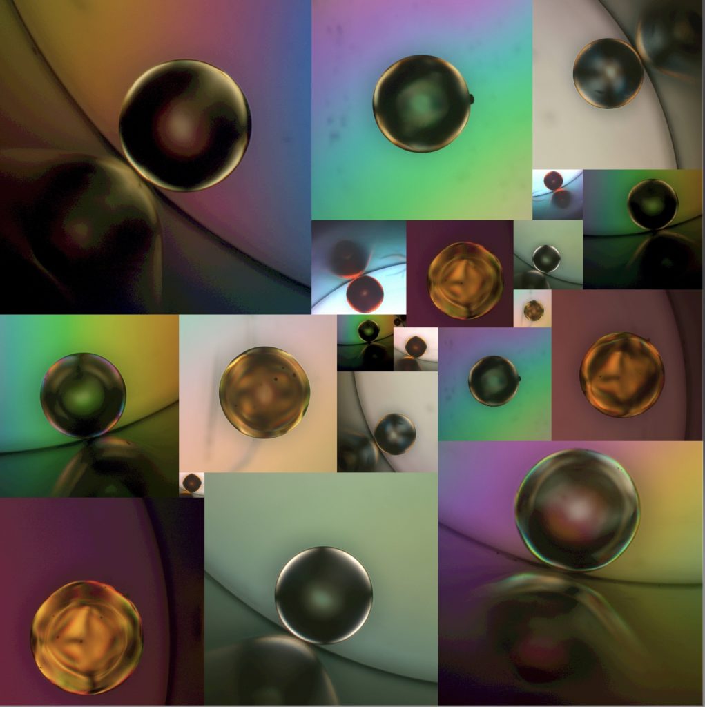
Submitted by Lukas Hackl and Mary Carmen Reid, a collage of optical microscope images taken of various ion-exchange resin beads used in water softening and purification (average diameter: ~500 μm). The images were not color-enhanced, light from the microscope’s illuminator is simply scattered by the beads and the microscope slide. Photoshop was used for arrangement into a “square of squares”: an integral square that is tiled using other, uniquely dimensioned squares.
The researchers integrate these ion-exchange beads into thin-film electrodes to capture select ions from a high-concentration influent stream (e.g. brackish groundwater) and to make freshwater. The ion-exchange resin electrodes are regenerated and reused electrochemically for cost-effective and efficient water desalination.
The research team consisted of Mary Carmen Reid (UC Berkeley), Lukas Hackl (UC Berkeley/LBNL), Jeffrey Urban (Molecular Foundry), and Ashok Gadgil (UC Berkeley). The image was taken using the Leica DM4500P Polarized Optical Microscope in the Foundry’s Organic and Macromolecular Synthesis facility.
In second place:
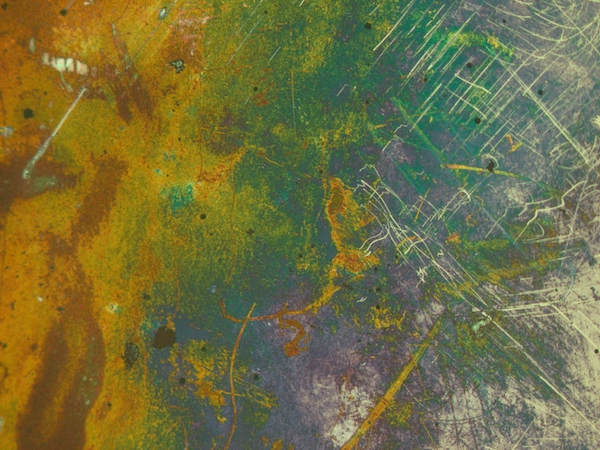
Submitted by Chris Anderson (UC Berkeley/Molecular Foundry), this image shows a redox-active covalent organic framework (COF) was grown on a glassy-carbon electrode. COFs are extended 2D or 3D organic polymers with some measure of crystallinity. The COF structure includes redox-active units called anthraquinones, and is grown on a conductive (1.5 cm x 1.5 cm) electrode. This COF was being tested as the active material in an electrochemical carbon capture device.
In third place:
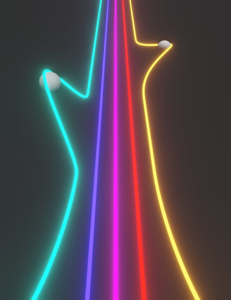
Submitted by Ruopeng Zhang, this artwork was designed to depict electrons pulling dislocation strings. It is designed for the article “Defect reconfiguration in a Ti–Al alloy via electroplasticity” published in Nature Materials. In this work, the researchers demonstrated that the application of an external electric current to a Ti-Al alloy could significantly alter the dislocation morphology during mechanical deformations. The technique we used has a potential to significantly reduce the cost of forming Ti-Al components.
The research team consisted of Ruopeng Zhang (UC Berkeley), Shiteng Zhao (UC Berkeley), and Andy Minor (UC Berkeley/Molecular Foundry).
In fourth place:
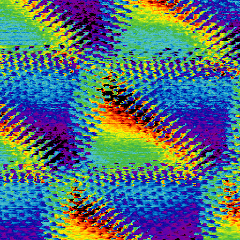
Submitted by Iqbal Bakti Utama, this image shows what happens when two monolayers with slightly mismatched lattice vectors are stacked together: the atoms can form an interference-like moiré pattern. Furthermore, if the misalignment is relatively small, the lattices may prefer to reconstruct into registry in stacking domains. Here, the researchers imaged the coexistence of moiré and reconstructed domains in a twisted double bilayer graphene on a boron nitride substrate.
The scanning microwave impedance microscopy (sMIM) provides a high sensitivity to probe the structure of moiré lattices and superstructures, including those at buried interfaces, with exquisite resolution even at room temperature. Thus, sMIM is ideal for characterizing van der Waals heterostructures, which are known to exhibit correlated electronic phenomena and topological physics that strongly depend on the structural details of the devices.
The research team consisted of Kyunghoon Lee, M. Iqbal Bakti Utama, and Salman Kahn of UC Berkeley.
In 5th place:
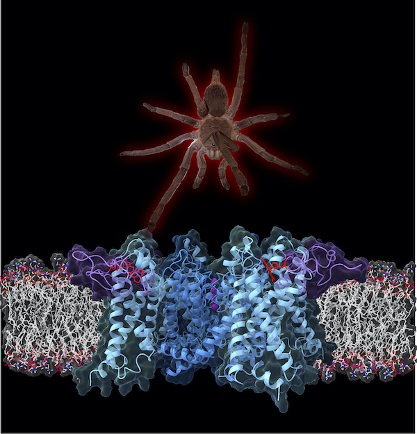
Submitted by Bruce Cohen, peptidyl toxins from the Chinese hissing bronze wolf tarantula Chilobrachys guangxiensis are labeled with new environment-sensitive fluorophores and used to image Kv2.1 channel conformational changes in live cells. Ion channels respond to membrane potential and control the electrical activity of neurons. Fluorescently labeled toxins are novel probes of voltage-gated ion channel structure and allostery.
The research team consisted of Bruce Cohen (Molecular Foundry) and Jon Sack (UC Davis). The image was featured as cover artwork in ACS Chemical Neuroscience.
In 6th place:

Submitted by Yin Liu, this is an SEM image of a twisted GeS crystal, a semiconductor material that, like graphene, readily forms sheets that are only a few atoms thick. To create the twisted structures, the team took advantage of a crystal defect called a screw dislocation, a “mistake” in the orderly crystal structure that gives it a bit of a twisting force forming and “Eshelby Twist”, named after scientist John D. Eshelby.
The work by this research team (Liu et al., 2019) was published in Nature.
Congratulations to all our winners, and thank you to all our entrants as well as all who voted! Stay tuned as we introduce more of the NanoArt as a new set of Zoom backgrounds and as backdrops to our 2021 NanoArt calendar!

