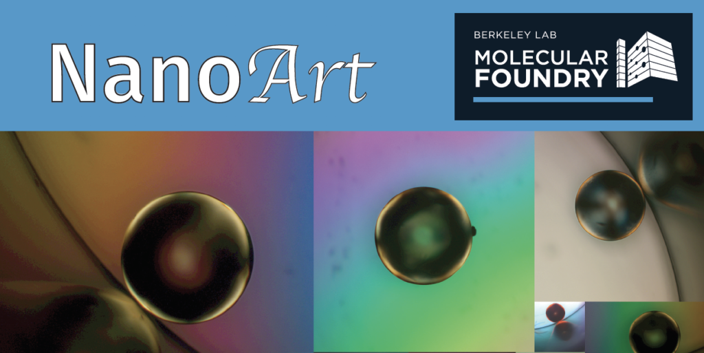
Have a very Nano New Year with the Molecular Foundry’s 2021 Calendar, featuring colorful submissions to the 2020 NanoArt Image Contest. The work behind these images comes from Foundry staff and users spanning all seven of the Foundry’s technical facilities.
Do you know which day is ‘DNA Day’? Check the Foundry calendar!
Download and print your own copy.
About the 2021 Calendar
January
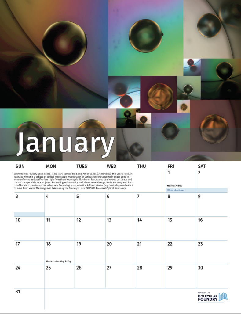
Submitted by Foundry users Lukas Hackl, Mary Carmen Reid, and Ashok Gadgil (UC Berkeley), this year’s NanoArt 1st place winner is a collage of optical microscope images taken of various ion-exchange resin beads used in water softening and purification. Light from the microscope’s illuminator is scattered by the ~500 μm beads and the microscope slide. In a project collaborating with Foundry staff, these ion-exchange beads are integrated into thin-film electrodes to capture select ions from a high-concentration influent stream (e.g. brackish groundwater) to make fresh water. The image was taken using the Foundry’s Leica DM4500P Polarized Optical Microscope.
February
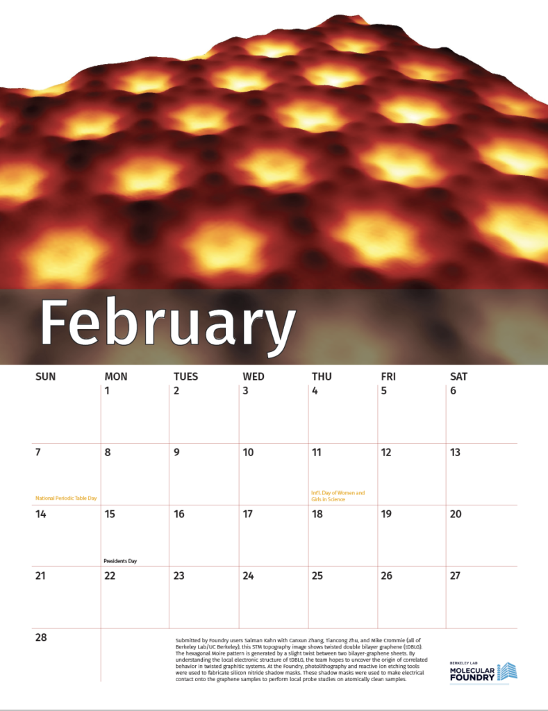
Submitted by Foundry users Salman Kahn with Canxun Zhang, Tiancong Zhu, and Mike Crommie (all of Berkeley Lab/UC Berkeley), this STM topography image shows twisted double bilayer graphene (tDBLG). The hexagonal Moire pattern is generated by a slight twist between two bilayer-graphene sheets. By understanding the local electronic structure of tDBLG, the team hopes to uncover the origin of correlated behavior in twisted graphitic systems. At the Foundry, photolithography and reactive ion etching tools were used to fabricate silicon nitride shadow masks. These shadow masks were used to make electrical contact onto the graphene samples to perform local probe studies on atomically clean samples.
March
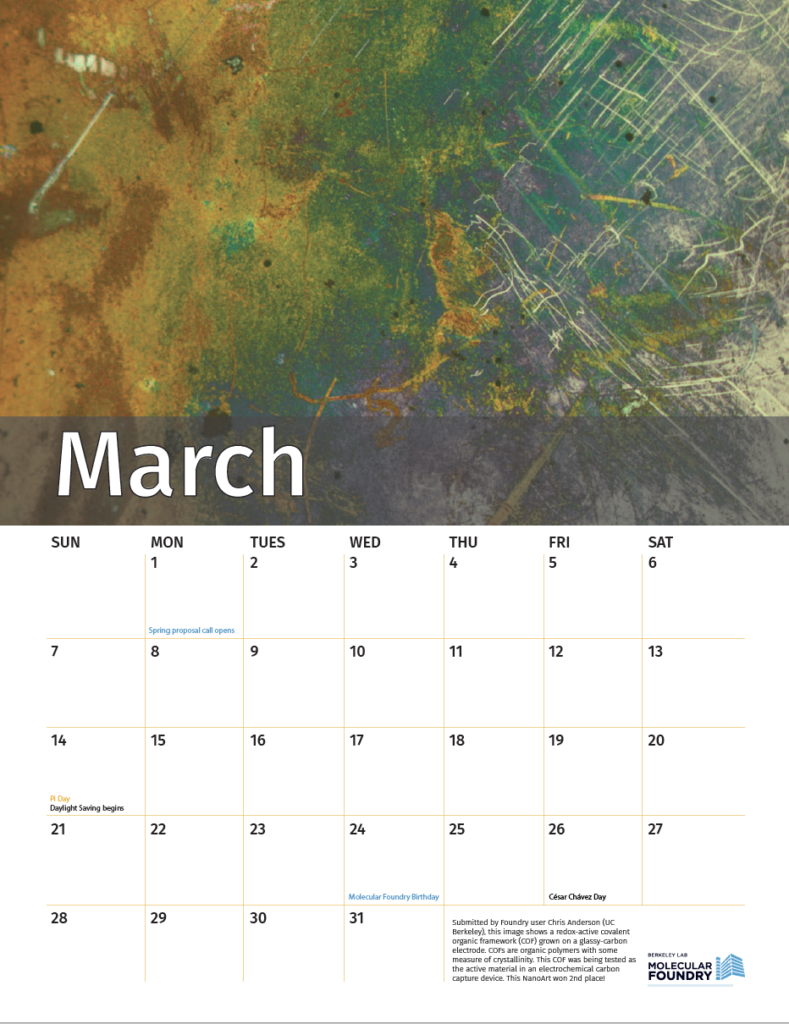
Submitted by Foundry user Chris Anderson (UC Berkeley), this image shows a redox-active covalent organic framework (COF) grown on a glassy-carbon electrode. COFs are organic polymers with some measure of crystallinity. This COF was being tested as the active material in an electrochemical carbon capture device. This NanoArt won 2nd place!
April
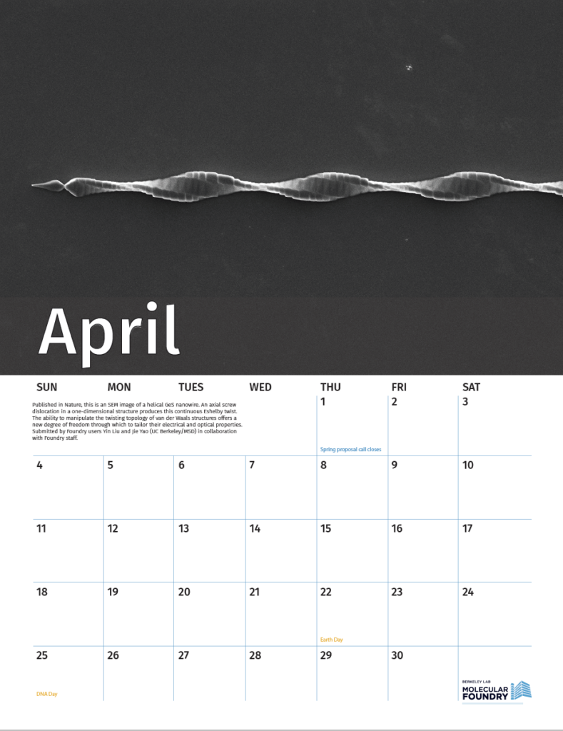
Published in Nature, this is an SEM image of a helical GeS nanowire. An axial screw dislocation in a one-dimensional structure produces this continuous Eshelby twist. The ability to manipulate the twisting topology of van der Waals structures offers a new degree of freedom through which to tailor their electrical and optical properties. Submitted by Foundry users Yin Liu and Jie Yao (UC Berkeley/MSD) in collaboration with Foundry staff.
May
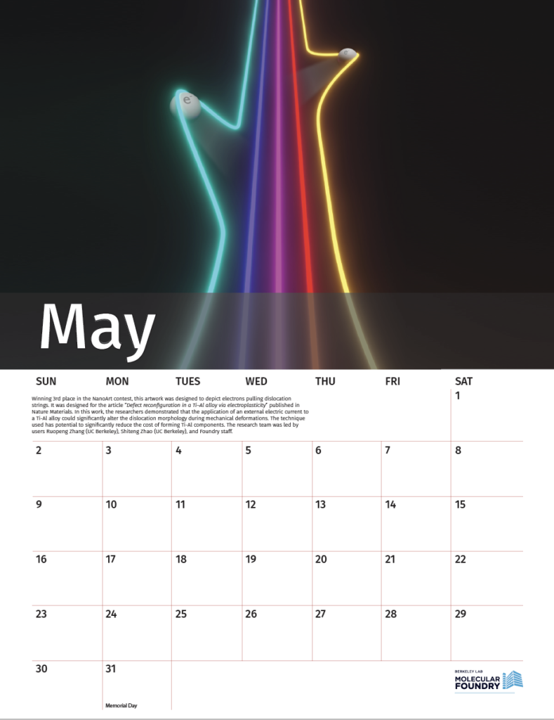
Winning 3rd place in the NanoArt contest, this artwork was designed to depict electrons pulling dislocation strings. It was designed for the article “Defect reconfiguration in a Ti–Al alloy via electroplasticity” published in Nature Materials. In this work, the researchers demonstrated that the application of an external electric current to a Ti-Al alloy could significantly alter the dislocation morphology during mechanical deformations. The technique used has potential to significantly reduce the cost of forming Ti-Al components. The research team was led by users Ruopeng Zhang (UC Berkeley), Shiteng Zhao (UC Berkeley), and Foundry staff.
June
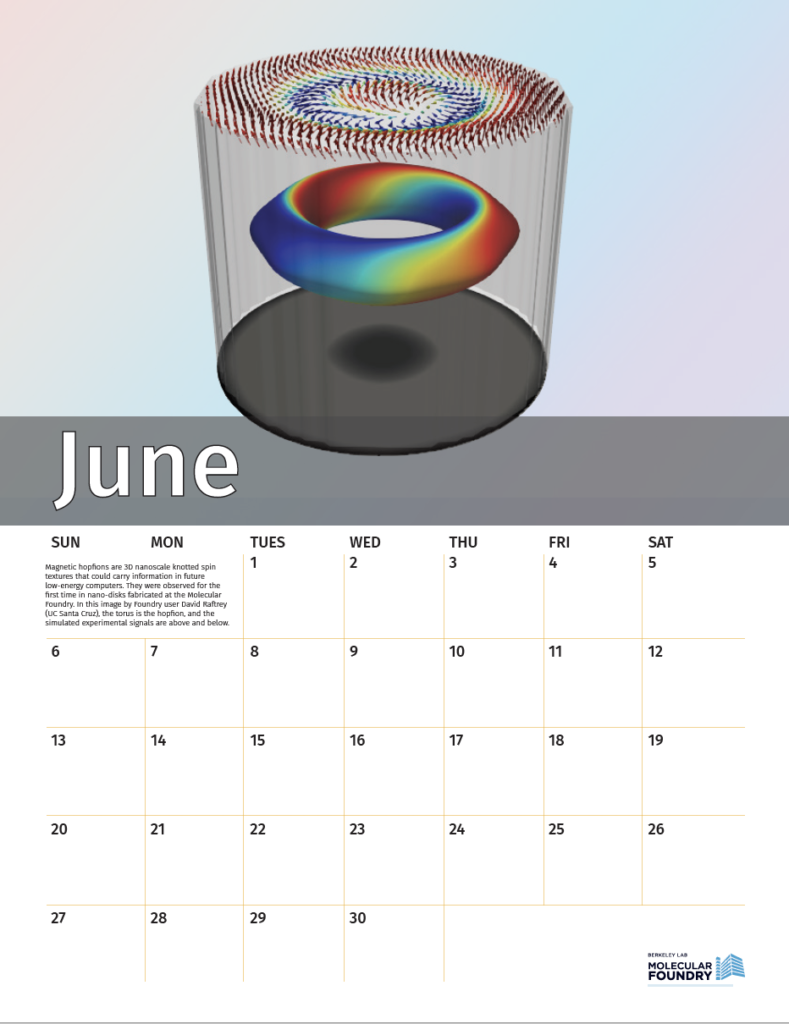
Magnetic hopfions are 3D nanoscale knotted spin textures that could carry information in future low-energy computers. They were observed for the first time in nano-disks fabricated at the Molecular Foundry. In this image by Foundry user David Raftrey (UC Santa Cruz), the torus is the hopfion, and the simulated experimental signals are above and below.
July
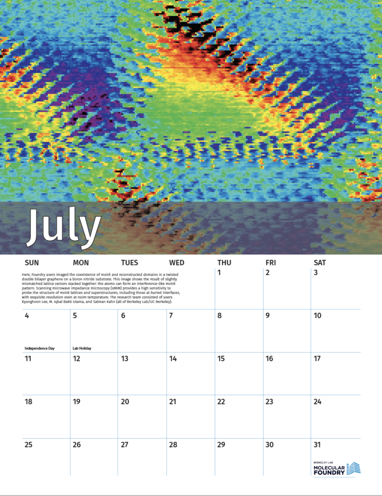
Here, Foundry users imaged the coexistence of moiré and reconstructed domains in twisted double bilayer graphene on a boron nitride substrate. This image shows the result of slightly mismatched lattice vectors stacked together: the atoms can form an interference-like moiré pattern. Scanning microwave impedance microscopy (sMIM) provides a high sensitivity to probe the structure of moiré lattices and superstructures, including those at buried interfaces, with exquisite resolution even at room temperature. The research team consisted of users Kyunghoon Lee, M. Iqbal Bakti Utama, and Salman Kahn (all of Berkeley Lab/UC Berkeley).
August
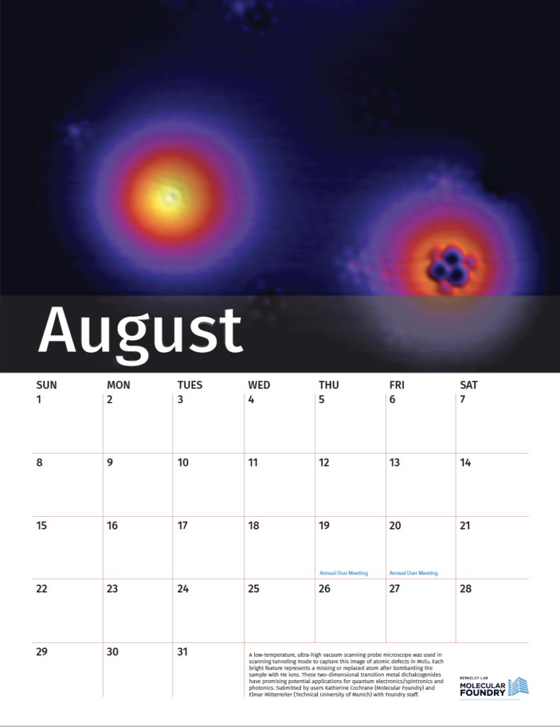
A low-temperature, ultra-high vacuum scanning probe microscope was used in scanning tunneling mode to capture this image of atomic defects in MoS2. Each bright feature represents a missing or replaced atom after bombarding the sample with He ions. These two-dimensional transition metal dichalcogenides have promising potential applications for quantum electronics/spintronics and photonics. Submitted by users Katherine Cochrane (Molecular Foundry) and Elmar Mitterreiter (Technical University of Munich) with Foundry staff.
September
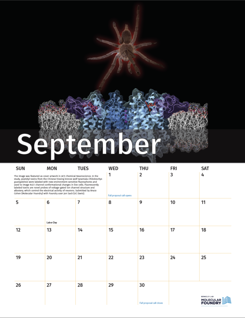
The image was featured as cover artwork in ACS Chemical Neuroscience. In the study, peptidyl toxins from the Chinese hissing bronze wolf tarantula Chilobrachys guangxiensis were labeled with new environment-sensitive fluorophores and used to image Kv2.1 channel conformational changes in live cells. Fluorescently labeled toxins are novel probes of voltage-gated ion channel structure and allostery, which control the electrical activity of neurons. Submitted by Bruce Cohen (Molecular Foundry) with Foundry user Jon Sack (UC Davis).
October
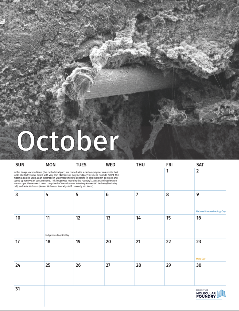
In this image, carbon fibers (the cyclindrical part) are coated with a carbon-polymer composite that looks like fluffy snow, mixed with very thin filaments of polymers (polyvinylidene fluoride PVDF). This material can be used as an electrode in water treatment to generate in-situ hydrogen peroxide and speed up removal of contaminants. This image was made by the Foundry’s Zeiss scanning electron microscope. The research team comprised of Foundry user Arkadeep Kumar (UC Berkeley/Berkeley Lab) and Nate Hohman (former Molecular Foundry staff, currently at UConn).

November
Simulation snowflakes! These are multi-slice simulated electron diffraction patterns for small nanoparticles of gold (Au) atop one or several layers of molybdenum disulfide (MoS2). Comparing the simulations to the experimental data allows us to study the interface of 2D semiconductors and metal contacts, and potentially control the electronic properties of these 2D materials at the nanoscale. Submitted by Foundry user Clarissa Bhargava (UC Berkeley), building on code written by Foundry staff.
December
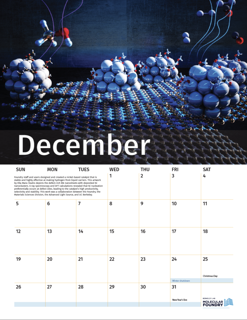
Foundry staff and users designed and created a nickel-based catalyst that is stable and highly effective at making hydrogen from liquid carriers. This artwork by Ella Maru Studio depicts the defect-rich BN nanosheets with deposited Ni nanoclusters. X-ray spectroscopy and DFT calculations revealed that Ni nucleation preferentially occurs at defect sites, leading to the catalyst’s high productivity, selectivity and stability. This work was a collaboration between the Foundry, the Materials Sciences Division, the Advanced Light Source, and UC Berkeley.

