Scientific Achievement
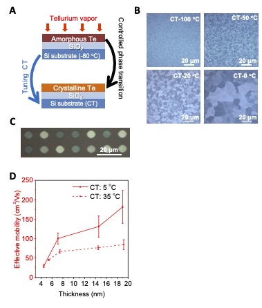
B: Polarized light microscopy images of the Te films (10 nm) crystallized at different crystallization temperatures (CT).
C: Polarized light microscopy image of the patterned 0 oC crystallized Te (10 nm) array with lateral dimension of 6 mm .
D: Thickness-dependent effective mobility for Te FETs crystallized at different temperatures.
Achieved Te thin films with large grains or single-crystal arrays by controlling the crystallization process during thermal evaporation.
Significance and Impact
This work provides a simple method to fabricate wafer-scale large grain Te thin films or single crystal arrays at near-ambient temperature, which have high effective hole mobility.
Research Details
- Visualized and modeled the kinetics and dynamics of the crystallization of thermally evaporated Te films.
- Low-temperature processing of highly crystalline tellurium films is demonstrated by controlling the crystallization process.

