The Molecular Foundry hosted it’s annual NanoArt competition in celebration of National Nano Day – 10/9 – which helps raise awareness of nanotechnology, how it is currently used in products that enrich our daily lives, and the challenges and opportunities it holds for the future.
We had a number of great entries from the Molecular Foundry community, and now the votes are in!
1st Place
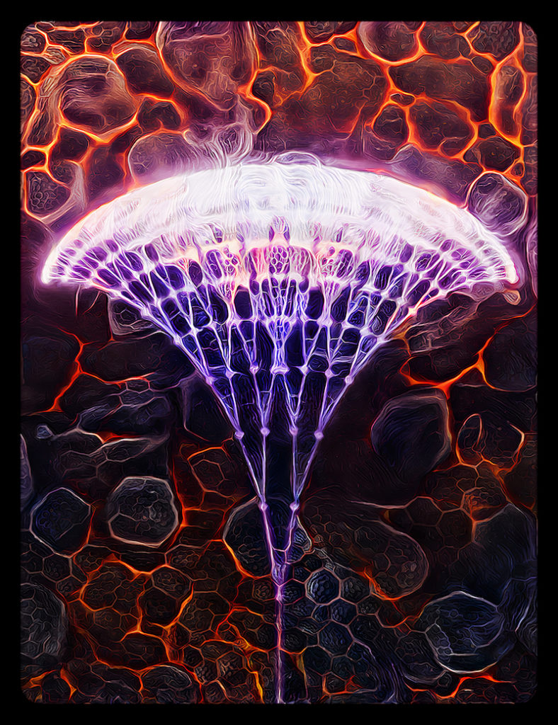
“Photon Avalanche” created by Mikołaj Łukaszewicz and Artur Bednarkiewicz and submitted to the contest by Bruce Cohen. Foundry users and scientists have created avalanching nanoparticles (ANPs), which exhibit true photon avalanching within a nanostructure at room temperature. ANPs have the most extreme non-linear optical response of any nanostructure and can be imaged in real time at deeply subwavelength resolutions using simple microscopy. The chain reaction-type light avalanching process is depicted in this artwork. ANPs will unlock a variety of optical applications from deeply sub-wavelength bioimaging to quantum sensing.
The artwork was an artistic rendering of work by Mikołaj Łukaszewicz and Artur Bednarkiewicz from the Institute of Low Temperature and Structure Research at Polish Academy of Sciences, Wroclaw, Poland, and Emory Chan and Bruce Cohen from the Molecular Foundry, published in Nature.
2nd Place
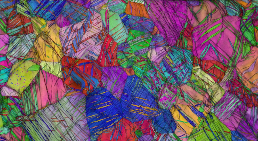
Submitted by Ruopeng Zhang. This image is an Electron Backscatter Diffraction (EBSD) orientation map of pure titanium with a nanotwinned structure. In the orientation map, each color represents a unique crystallographic orientation of the grains. The thin strips reveal the nanotwinned structure produced via a multi-step cryo-forging process carried out in liquid nitrogen followed by annealing at 400˚C. As a result, the processed material exhibits outstanding mechanical properties of both ultrahigh strength and ductility, especially at cryogenic temperatures. The processed high-purity Titanium exhibits outstanding mechanical properties of both ultrahigh strength and ductility, especially at cryogenic temperatures. This design strategy demonstrated the potential of achieving desired mechanical properties solely through microstructure engineering and without changing the composition of the materials. With this finding, it is possible to develop future structural materials with better performance and much reduced environmental footprint.
The image was collected as part of work conducted by Ruopeng Zhang, Shiteng Zhao, and Andrew M. Minor, which was published in Science.
3rd Place
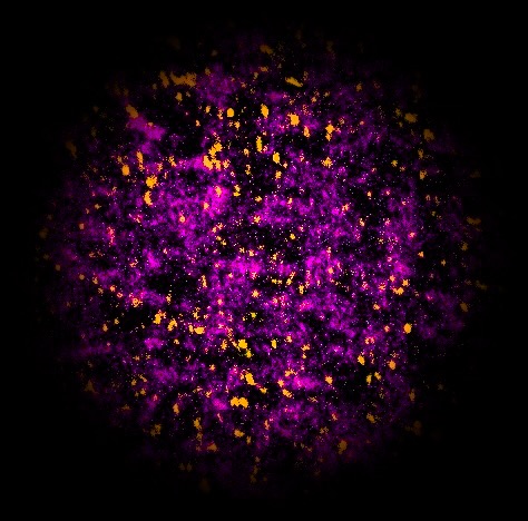
Submitted by Tim Kodalle. Photoluminescence imaging was used to probe 2D/3D halide perovskite films. The bright orange features stem from the luminescence of the 2D bulks on the surface of the 3D film (purple luminescence). Bulky 2D halide perovskites are used as surface treatment on 3D perovskites to enhance stability and reduce surface related recombination losses. PL-Imaging helps us to understand the distribution of the 2D bulks. These materials can be used to enhance the stability and efficiency of perovskite solar cells.
The image was produced as part of work conducted by Vivian Meier, Tim Kodalle & Carolin Sutter-Fella.
4th Place
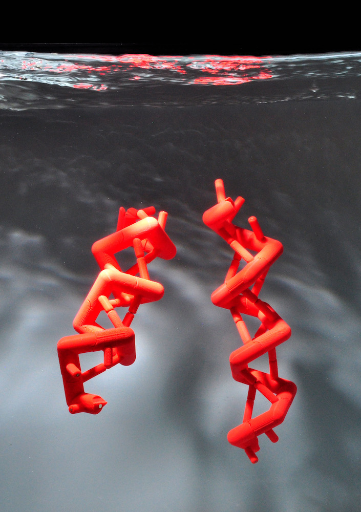
Submitted by Ron Zuckermann. 3D-printed atomic models of amino acids, the fundamental building blocks of all proteins, spontaneously assemble into stable alpha helices in the Foundry circulating water self-assembly tank. Weak magnetic interactions, and shape complementarity between pieces, directs the assembly of helices through only random collisions. The design and synthesis of self-assembling materials requires an intuitive understanding of the complex balance between entropy, enthalpy, kinetics and thermodynamics. This representation of how a stable protein secondary structure can spontaneously form allows one to observe details of the assembly pathway and most importantly how multiple weak interactions cooperate with one another to create a persistent assembly.
The photo was taken by Ron Zuckermann and Uyen Nguyen as part of work published in 3D Printing and Additive Manufacturing.
5th Place
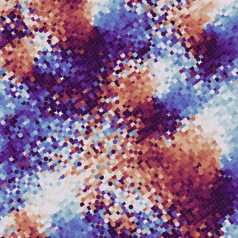
Submitted by Sean Mills. Atomic dislocations leave an impression. This type of imaging, done with the Foundry’s TEAM 0.5 microscope, enables researchers to observe atomic scale defects found in next generation nuclear materials.
6th Place
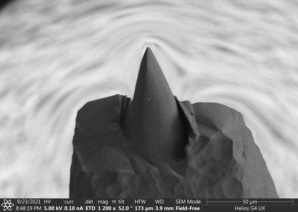
Submitted by Alexander Stibor. Electron microscopy image of a niobium nanotip that is electrostatically charged, creating a field that distorts the pathways of the scanning electron beam. This produces a visible lensing effect around the tip. Alexander Stibor and Cameron Johnson are developing superconducting niobium nanotip field emitters for better electron beam sources for microscopy, spectroscopy and quantum information science.

