By Temme von Lackum Dedlow
The last decade has seen extraordinary advancements in electron microscopy, enabling researchers to image materials at increasingly high resolutions. This type of high-resolution imaging, which allows us to “see” structures down to individual atoms, is still limited by the difficulty of visualizing and classifying movements of atoms within the material. A years-long collaboration of international Foundry users from research and industry, including Foundry staff scientist Christian Kisielowski, has created a new imaging procedure that can provide information about the movement of atoms in a material without sacrificing resolution. Their work was published in Nature Communications.

In the past, when using data to reconstruct 3D images of the atoms in a material, atoms have been treated as static within the structure, with a certain amount of blurring due to consistent, temperature-dependent vibrations. But this assumption makes it difficult to identify atoms that have moved or been displaced during the imaging process.
In transmission electron microscopy (TEM), which relies on a beam of electrons passing at very high speeds through a very thin sample, understanding how the beam interacts with the sample can be critical to correctly interpreting the resulting data. This is especially important when researchers are trying to make determinations about the functional behavior of the material. The surface atoms of a material, as the first plane of interaction with the environment, are key in determining these functional properties and especially susceptible to disturbance—including that caused by the electron beam during microscopy.
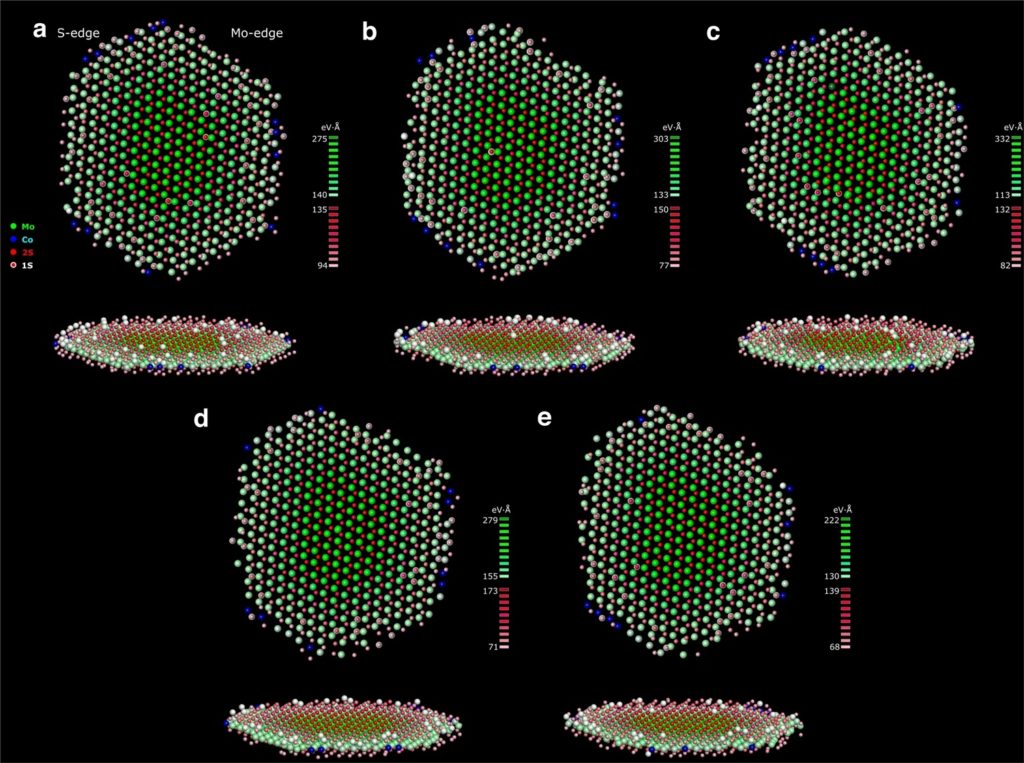
The research team used the National Center for Electron Microscopy’s TEAM 0.5 microscope to carry out experimental measurements of a nanocrystal composed of cobalt, molybdenum, and sulfur, a well-studied catalytic material with important industrial applications. Their analysis showed displacement of atoms at the edges of the nanocrystal due to interaction with the electron beam. By applying the new procedure to the collected data, the researchers were able to recover the pristine structure of the material: that is, to identify and locate the atoms in the nanocrystal, including those at the disturbed edges.
Interested in Becoming a Foundry User?
Join our collaborative, multidisciplinary environment.
Learn more >
Looking forward, this work—which expands existing capabilities for time-resolved 3D imaging—also has important applications for observing material behavior in real time. For chemical processes, the relevant time scale varies by many orders of magnitude, but as technology improves, the researchers have their sights set on time-resolution down to pico- and femtoseconds (i.e., billionths and quadrillionths of a second) while maintaining atomic resolution. This is the scale on which electronic processes take place, and has exciting implications for our ability to measure and observe quantum phenomena.
“The nature of scientific funding can make it difficult to carry out this kind of explorative research since it relies on a combination of highly specialized equipment, international expertise, and years of collaboration,” said Kisielowski. “But the instrumentation and research infrastructure of the Foundry, in combination with the collaborating institutions, provided a unique opportunity for access and support that made this work possible.”
The other collaborators on this work include Fu-Rong Chen of Hong Kong City University, Dirk van Dyck of the University of Antwerp, Lars P. Hansen of Haldor Topsøe, Bastian Barton, also of LBNL, and Stig Helveg of the Technical University of Denmark.

