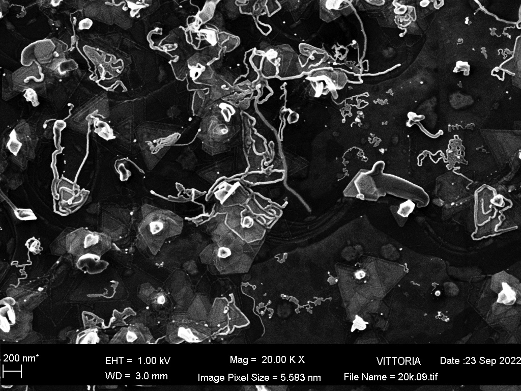
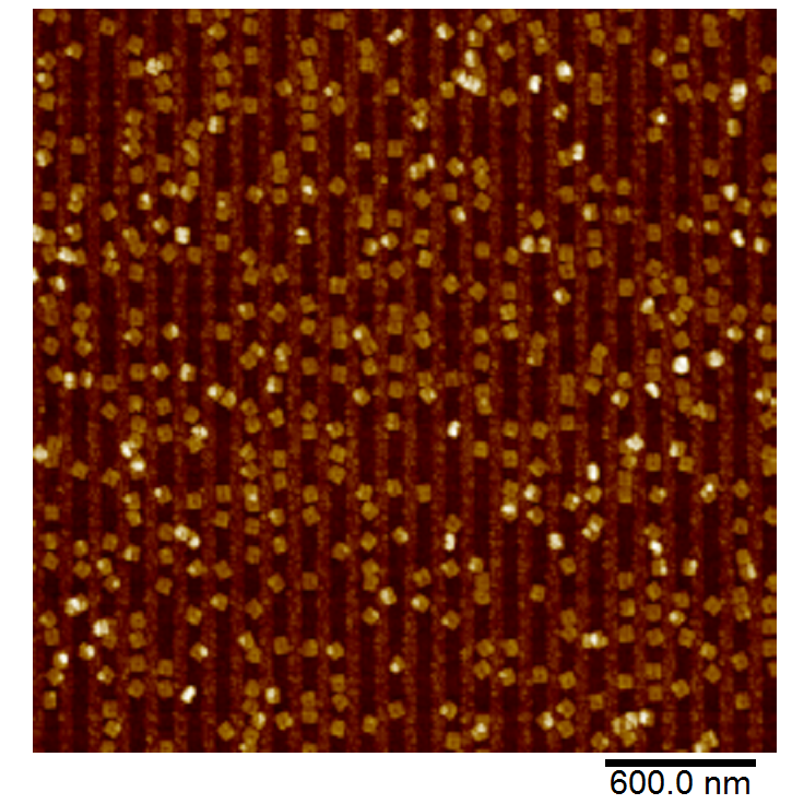
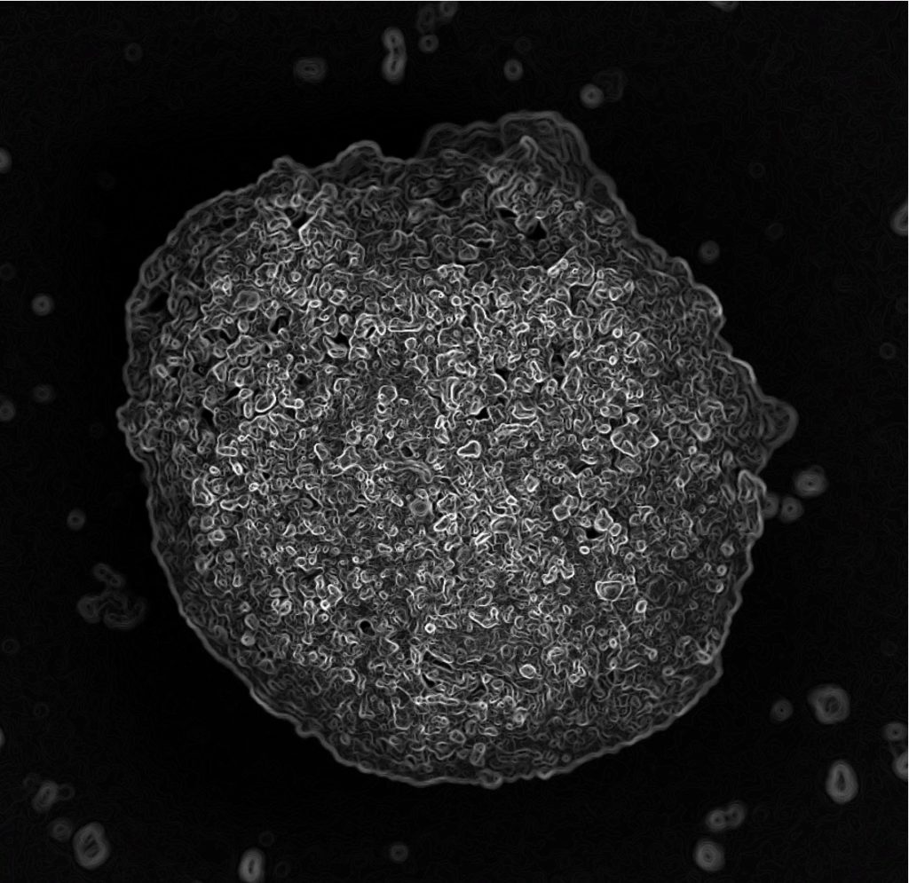
The Molecular Foundry hosted it’s annual NanoArt competition in celebration of National Nano Day – 10/9 – which helps raise awareness of nanotechnology, how it is currently used in products that enrich our daily lives, and the challenges and opportunities it holds for the future.
We had a number of great entries from the Molecular Foundry community, and now the votes are in!
1st Place
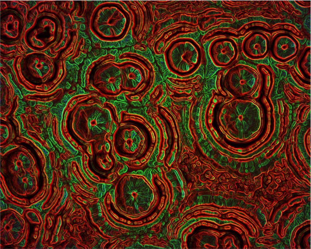
Flower-like halide perovskite crystals submitted by Maged Abdelsamie, and part of work done by Mriganka Singh, Maged Abdelsamie, and Carolin Sutter-Fella. This material is used in the development of new solar cells.
2nd Place
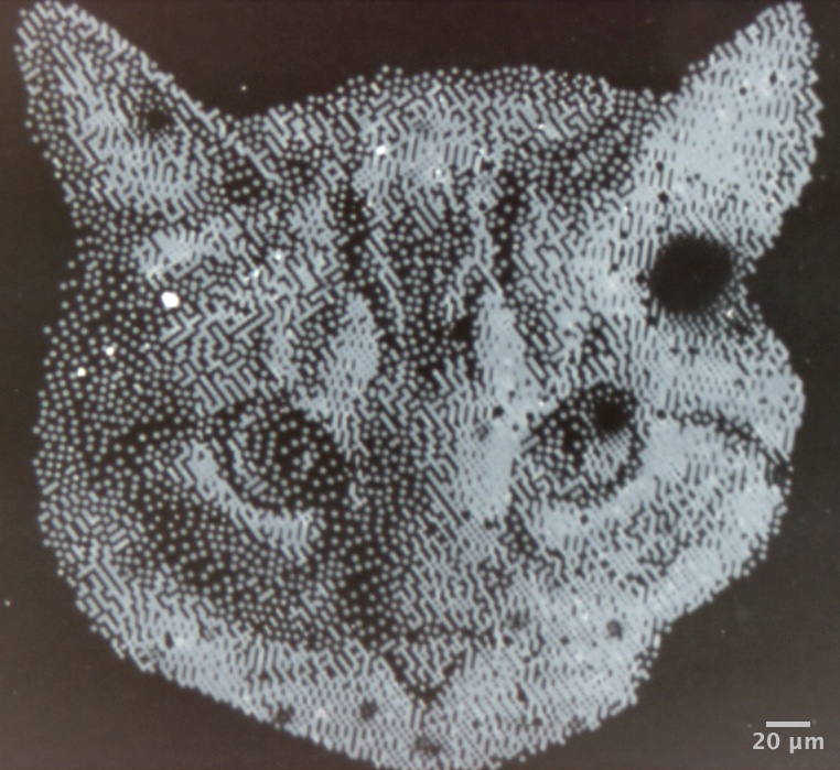
Submitted by Jia-Ahn Pan. The “Upconverting Nano-Micro Cat” was fabricated by depositing upconverting nanoparticles in a specific micro-scale pattern. These upconverting nanoparticles convert infrared light into visible light and are used for many optical applications. Each bright pixel on the image is made up thousands of these nanoparticles that were precisely placed using a light-induced chemical reaction. This technology could be used to make better optical and optoelectronic devices (e.g., lasers, detectors).
The image was collected as part of work conducted by Jia-Ahn Pan and Emory Chan.
3rd Place
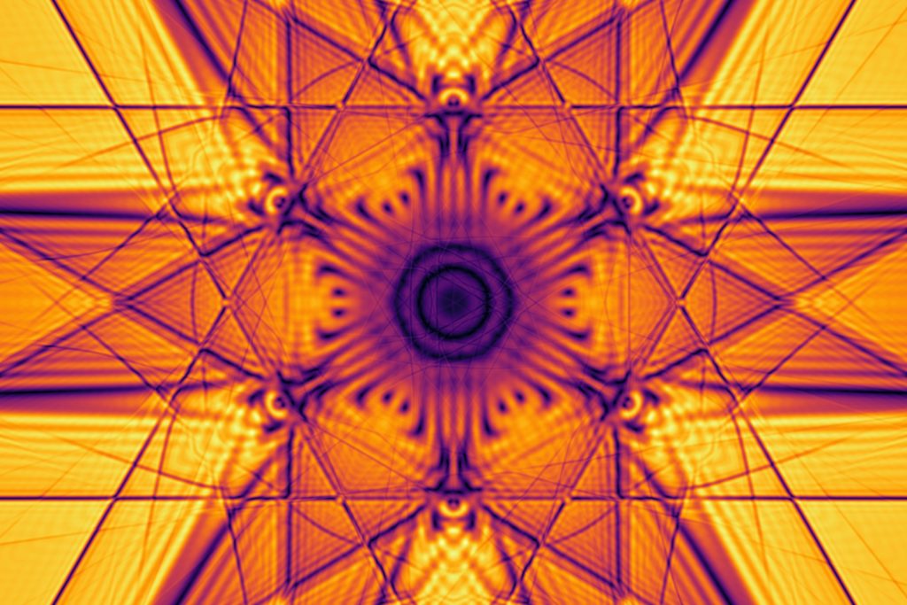
Submitted by Steven Zeltmann. This is a simulation of a large-angle converged beam electron diffraction experiment performed on a silicon crystal. The web of criss-crossing lines that run through the pattern carry detailed information about the structure and symmetry of the crystal. Researchers can use these simulations to help determine the precise structure of nanomaterials, such as during the process of fabricating novel nanoscale materials.
4th Place
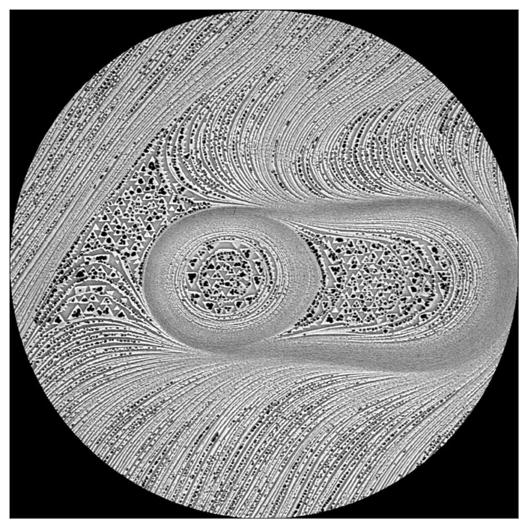
Submitted by Cameron Johnson. Monolayer (triangles) and bilayer (black spots) of cobalt on the atomic terraces of a single crystal ruthenium(1000) surface, grown in situ and imaged using low energy electron microscopy. The image field of view is 10 micrometers. Using the Foundry’s qSPLEEM, images like this offer improved resolution and understanding of the growth and structure of thin magnetic films.
This image was collected as part of work done by Juan De La Figuera, Instituto de Química Física Rocasolano; Sandra Ruiz Gomez, Max Planck Institute for Chemical Physics of Solids; Cameron Johnson, Molecular Foundry; Alexander Stibor, Molecular Foundry; Andreas Schmid, Molecular Foundry.
5th Place
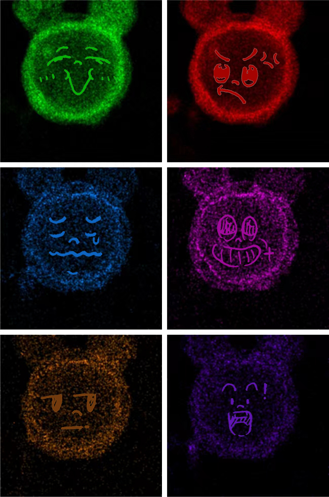
Submitted by Chaochao Dun. As a highly disordered multicomponent system, the high-entropy ceramic (reflected here by EDS-Mapping like (CoNiCuZnAl)Ox) provides many fascinating properties, like sluggish kinetics, heavy lattice distortions and abundant oxygen vacancies, and many unexpected catalytic properties emerge by turning the elemental compositions and ratios. This material could be used for the dry reforming of methane.
6th Place

Submitted by John C. Thomas. A schematic depicting tunneling electron-induced photon emission from a single sulfur vacancy within monolayer tungsten disulfide. The scanning tunneling microscope is capable of resolving photons emitted at the atomic scale, due to tunneling-induced luminescence. It’s used to observe quantum interactions at the atomic-scale.
This image was created as part of work done by Bruno Schuler, Katherine Cochrane, Molecular Foundry John Thomas, and Alexander Weber-Bargioni published in Science Advances.
Honorable Mentions
