By Alison Hatt

A team of researchers at the Molecular Foundry has optimized a technique for exploring interactions between light and electrons happening deep inside semiconductor materials, visualizing the details with nanoscale precision. Their approach can provide new insights into the physical properties that underpin modern semiconductor technologies.
Leveraging their expertise in fabricating two-dimensional materials and their heterostructures, the team systematically studied the impact of sample design on the spatial resolution of cathodoluminescence (CL) microscopy. They also established a lower limit for the diffusion length of excited charge carriers in hexagonal boron nitride (hBN), a popular encapsulating medium for semiconductors, providing the first estimate of that critical property. The study appeared earlier this year in a special issue of the journal Nanoscale highlighting early career researchers.
“We’re showing how designing your buried interface or nanoscale heterostructure can strongly impact spatial resolution and brightness in cathodoluminescence,” said Archana Raja, who led the study, “and we’ve explained this in a 2D heterostructure stack, which is a very popular geometry. Encapsulating atomically thin materials in hBN is all the rage and we’re discovering how excited charge carriers flow through it.”
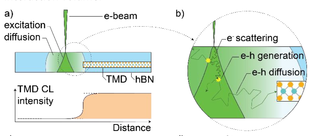
In CL microscopy, researchers shine a beam of electrons on a sample, which creates pairs of electrons and holes (the empty spots where electrons used to be) in the material. Those pairs of electrons and holes are known as excitons, and they can travel some distance in the material before recombining and emitting light, which is then detected by the researchers. The emitted light provides information about how electrons and holes (known as charge carriers) behave in the material, helping researchers understand fundamental material properties and design technological devices.
Buried interfaces abound in nanostructured materials, such as between the layers in stacked structures or between quantum dots or nanowires embedded in an encapsulating matrix. Very often, the useful or interesting properties of these structures arise from the interfaces where different materials meet, which motivates scientists to characterize and understand them.
Interested in Becoming a Foundry User?
Join our collaborative, multidisciplinary environment.
Learn more >
CL microscopy is a powerful technique for these types of systems because it can penetrate deeper into a material and with higher resolution than what is typically possible with light-based microscopy techniques.
For this study, the Foundry team prepared a series of precisely layered structures where atomically thin layers of a transition metal dichalcogenide (TMD) were sandwiched between encapsulating layers of hexagonal boron nitride. TMDs are semiconductors with useful optoelectronic properties and hexagonal boron nitride is a popular encapsulating material used to protect and passivate nanoscale semiconductors in devices. The team prepared a series of samples in which the top layer of hBN varied in thickness from 20nm to 330nm and then used CL microscopy to study the effect of the top-layer thickness on the diffusion of excitons in the material.
The team found that as they increased the thickness of the hBN layer, the emitted light got brighter but the spatial resolution deteriorated. They determined that an optimal balance of brightness and resolution was achieved with encapsulating layers around 100nm. “Researchers can use this information to image buried interfaces with better spatial resolution by knowing how the heterostructure they design impacts that resolution,” said Raja.
As a by-product of this study, the researchers were also able to determine a lower limit of about 200 nm for how excitons diffuse through hBN. To their surprise, they found the diffusion of excitons with the hBN appeared to be isotropic (the same in all directions) despite the fact that the 2D sandwich structures were highly anisotropic.
“This work really highlights our facility’s CL instrument as it relates to 2D heterostructures, which are a growing part of our Foundry user program,” said Raja. “At the Foundry, users can also synthesize nanostructures like quantum dots or use top-down nanofabrication to pattern 1D or 2D interfaces, and then they can also image such structures with the appropriate resolution, like we have shown with CL microscopy.”
Raja noted that the Foundry’s CL techniques are also well suited for studying the temperature dependence of buried interface properties. She pointed to the Foundry’s complimentary expertise in near-field optics, a characterization technique that can enable similar investigations but is better suited for certain types of samples. “There’s a unique environment at the Foundry that enables this kind of work, where we have all these techniques and capabilities in one place and have the students and postdocs and PIs interacting and working together.”
Using the CL tool, Foundry researchers and users are now exploring other sample structures, like 1D interfaces of TMDCs, and looking at color-centers or optically active defects in materials.
“We’re excited to offer users this ability to visualize optoelectronic processes such as exciton diffusion with nanometer-scale resolution in bulk-like materials and heterostructures,” said Alex Weber-Bargioni, Director the Molecular Foundry’s Imaging Facility. “Visualizing those processes below the surface with this kind of resolution is not possible with any other technique, to my knowledge, and there’s huge potential for what people can do with it.”

