By Alison Hatt

Electron microscopy and spectroscopy techniques are instrumental to our understanding of matter at the nanoscale and have fueled discoveries in nearly every field of science and technology. At the heart of each of these tools is an electron source, producing a beam of electrons used to probe and interrogate samples, and the instrument’s power and resolution depend, in part, on the quality of that source.
Now, researchers working at the Molecular Foundry have developed a new electron source that out–performs existing sources by more than an order of magnitude. Their results, which appeared in Physical Review Letters, may enable new fields in electron-based imaging and analysis and facilitate research in quantum information science.
“Optics and other components of electron microscopes have improved a lot in the last ten years, but it’s all only as good as the electron sources,” said project-lead Alexander Stibor, from the small company Electron Optica. “If you have a good beam from the beginning, you have a much easier job to optimize it.”
The project is a collaboration between researchers from industry, academia, and Foundry staff, performed through the Molecular Foundry’s user program, and supported in part by a Small Business Innovation and Research grant from the Department of Energy.
The team worked with what’s known as a field-emission electron source, in which an electric field is applied to a sharp metallic tip, causing it to emit a beam of electrons. Those electrons don’t all have the same energy, and the range of energies in a beam is known as its energy distribution. The narrower the energy distribution, the higher the resolution at which a beam can probe a material.
Here, the team used a trick from quantum mechanics to dramatically improve the energy resolution of their electron source, which is cooled to extremely low, superconducting temperatures.
“The idea is that you leverage the quantum nature of the emitter and the electrons to get a high-quality beam,” said Stibor. “We created a tip so small that only one quantum energy level can fit in it. Electrons coming out of the tip have to tunnel through this quantum level, and this means the beam has a very small energy distribution.”
Interested in Becoming a Foundry User?
Join our collaborative, multidisciplinary environment.
Learn more >
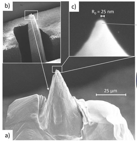
To achieve this feat, the researchers first had to solve the puzzle of how to fabricate a nano-sized field-emission tip. The team shaped a monocrystalline niobium wire into a sharp tip using electrochemical etching and focused-ion-beam milling, producing a smaller-than-usual electron microscopy tip. They then created a nano-sized protrusion on the apex using thermal annealing techniques, fabricating a tip with a radius of just 1.5 nm.
Not only does the resulting beam have a narrow energy spread, but it also retains a small emission angle and high intensity, unlike conventional techniques for filtering electron energies, allowing for an improved signal-to-noise ratio and enabling novel spectroscopic techniques.
The performance of the resulting superconducting nanotips was outstanding, with an energy distribution width of 60 millielectronvolts and excellent stability and brightness. The team played further quantum-mechanical tricks to tune to beam, applying a small voltage to reduce the energy distribution even further, down to 16 millielectronvolts or about twenty-times smaller than conventional electron sources.
Characterizing the nano-tips required the team to build a custom tool that could perform a variety of analytical techniques without removing the nanotip from a high-vacuum environment. The unit they created includes separate stations for measuring energy distribution, beam intensity, and electron correlation and is now available to researchers through the Foundry’s user program.
“Not only did we demonstrate the incredible performance of this electron source, but the project also established a facility at the Foundry for testing electron sources,” said Andrew Minor, Director of the Foundry’s National Center for Electron Microscopy. “This could benefit fields like ultrafast electron microscopy, where researchers are working to enhance the brightness of their sources and need to characterize them in an isolated environment.”
The choice of niobium for the nanotip was driven by the team’s interest in producing pairs of correlated electrons for quantum information science. The researchers initially hoped to find that electrons emitted from the superconducting source were correlated, maybe even entangled, as has been predicted by theorists, but measurements at the Foundry could not confirm the theory. Addressing this challenge is the subject of ongoing research, as is the development of other microscope components that can operate at low temperatures.
“This work is part of our larger effort to develop a low-temperature electron microscope, where the entire instrument operates at very low temperatures to achieve incredible resolution,” said Minor. “It’s complimentary to other recent work of ours with superconducting lenses for EM. Our great strength at the Foundry and across Berkeley Lab is our people and their ability to build the technologies we need to push this field into the next generation.”
Related Comment Article published in “Physics”

