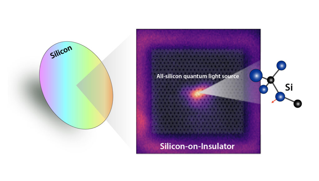
Adapted from this Berkeley Engineering press release

Quantum cryptography, if it could be achieved, would provide unparalleled levels of data security against nefarious hackers. That’s because quantum information can be encoded in photons — single particles of light — that can’t be copied or measured. Interlopers would be exposed immediately.
One of the high hurdles for quantum cryptography that scientists must first overcome, however, is the ability to create photons in ways that would reliably feed quantum networks, or a quantum internet.
Now, a team of researchers led by Boubacar Kanté, Foundry user and Chenming Hu Associate Professor in UC Berkeley’s EECS Department and faculty scientist at the Materials Sciences Division, has demonstrated the first on-demand quantum light source using silicon. Kanté says silicon — the material upon which millions of tiny electronic devices are manufactured each day — is the most “scalable” optoelectronic material known.
Their research was published in Nature Communications.
“The possibility to use silicon as a source of quantum light signifies that current large-scale Complementary Metal-Oxide Semiconductor (CMOS) chip manufacturing processes at the core of today’s optoelectronics and artificial intelligence (AI) devices may be directly used for future quantum systems,” Kanté said.
A quantum internet at scale, Kanté explained, would require not only a bright and efficient quantum light source but also photons that can propagate in existing optical fibers without being absorbed. No light source available today can meet that high bar. All require energy conversion for integration with CMOS compatible platforms, like what happens today with integrated “classical” light sources.
The on-demand silicon quantum light source developed by the UC Berkeley/Berkeley Lab team is the first experimental work demonstrating integration of a single silicon atomic emissive center, known as the G center, directly in a silicon nanophotonic cavity, Kanté explained.
“In this work, we successfully embedded for the first time an atomic defect in silicon the size of atoms (1 angstrom) in a silicon photonic cavity (1 micron) with the size of less than one-tenth of a human hair. The cavity forces the atom to be brighter, and it emits photons at a faster rate. Those are necessary ingredients for scalable quantum light sources for the future [quantum] internet,” he said.
Interested in Becoming a Foundry User?
Join our collaborative, multidisciplinary environment.
Learn more >
The Foundry was pivotal in determining the mechanisms behind this brightening process. “My research group at the Foundry performed first-principles calculations of the dipole moments of the single-photon emitters. These calculations were essential for showing that the alignment of the dipoles with the nanocavity polarization led to the large brightness enhancement,” said Foundry staff scientist Liang Tan.
Successful manufacturing of the single-photon emitters took place in cleanrooms at the Foundry and involved a controlled fabrication sequence, starting with a commercial-grade silicon wafer that is carbon implanted. The implantation was followed by lithography, etching and thermal annealing — all standard processes available in today’s semiconductor foundries.
The challenge, Kanté said, resided in creating atomic emissive centers and controlling their density and distribution for successful overlap with optical cavities. The team has overcome some of the key challenges, but improvements are needed, and many questions are yet to be answered.
Using silicon has been somewhat counterintuitive, said Walid Redjem, a postdoctoral research fellow in Kante’s group. “Silicon is what you call an indirect bandgap semiconductor. That means it is not favorable for light emission. For example, there is no efficient laser using silicon.”
But it turns out that reality only applies to classical light sources. “It’s not a problem for quantum light sources,” Kanté said. He and his team are already hard at work further refining their all-silicon quantum light source.
Read the full press release

