By Alison Hatt

Knowing the identity and 3D location of every atom in a material is a holy grail for nanoscience researchers. Armed with that information, the atomic-scale origins of measured properties could be directly interpreted, giving researchers awesome power to understand and engineer new materials. Current electron microscopy techniques can provide pieces of the puzzle, but none can simultaneously resolve both heavy and light atoms in complex nanostructures with atomic precision.
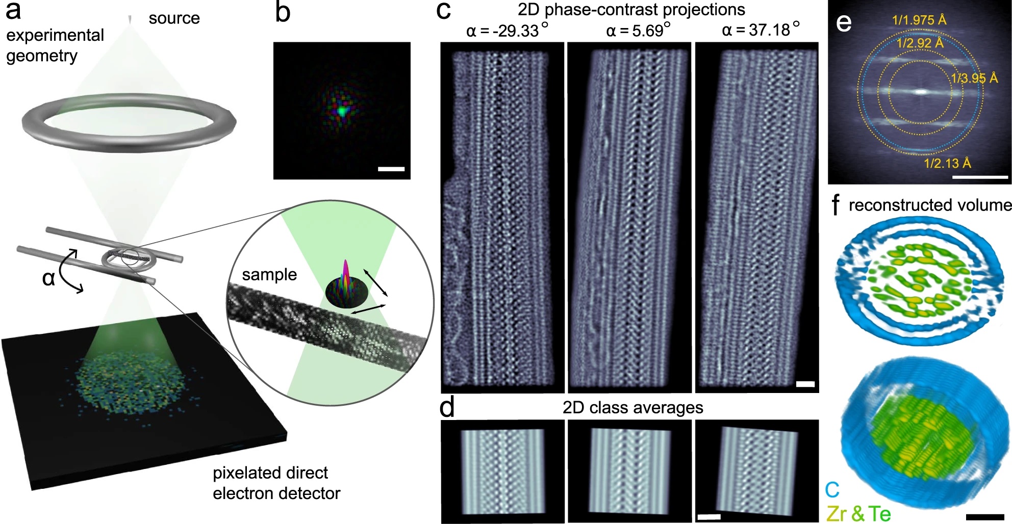
A new technique developed by a team of Molecular Foundry staff and users may change all that. Known as ptychographic atomic electron tomography (PAET), the technique combines two cutting-edge microscopy methods to provide ultra-precise, three-dimensional images of complex nanostructures containing both heavy and light atoms. They debuted the technique by imaging a particularly complicated sample of Zr-Te encased in a carbon nanotube.
“This work is both a breakthrough in methodology and solves a real material science question about the structure of a very complex nanostructure,” said Colin Ophus, a staff scientist in the Foundry’s NCEM facility and one of the lead investigators. The results appeared in Nature Communications.
The PAET technique is based on atomic electron tomography (AET), in which a series of 2D images is taken of a sample at various angles and then used to reconstruct the 3D image. The 2D images for AET are usually taken with HAADF-STEM, a high-resolution electron microscopy technique capable of resolving the positions of heavy atoms, while light atoms remain invisible.
In PAET, the team essentially performs AET but takes each of the 2D images using ptychography instead of HAADF-STEM. In ptychography, a series of electron-diffraction patterns is taken while scanning across a sample and are then used to reconstruct a 2D image with ultra-precise positions of both heavy and light atoms. Combining ptychography with AET, each of which are formidable on their own, required technical feats of alignment and optimization as well as advances in computation and data-processing to determine the 3D structure from millions of diffraction patterns. The result is an unprecedented view of a complex nanostructure that couldn’t be achieved with existing methods.
“Unlike all previous AET studies using HAADF-STEM, PAET can image single light elements like carbon and oxygen – which are important!” said Ophus. “What’s more, it’s also about ten times more electron-dose efficient than HAADF-STEM, causing far less sample damage, and allowing us to image thinner samples.”
Interested in Becoming a Foundry User?
Join our collaborative, multidisciplinary environment.
Learn more >
The team demonstrated the PAET technique by imaging a sandwich-like Zr11Te50 structure encapsulated in a double-walled carbon nanotube. The sample was chosen for its structural complexity, which couldn’t possibly be solved from a 2D projection, and its combination of heavy and light atoms. Their results provide atomic details for the entire nanostructure and identify a previously unknown ZrTe2 structure.
The team’s reconstruction and structure-determination process leveraged an arsenal of python codes developed by former Foundry postdoc Philipp Pelz for ptychographic image processing. Many of these methods are now available through the open-source software package py4DSTEM, which was recognized with an R&D 100 award last year. As they solved the atomic structure, the team also used density functional calculations to validate and refine their results, confirming the stability of the structure and exploring its electronic properties.
A key innovation underpinning this work is the 4D CAMERA detector, a superfast electron detector developed by Berkeley Lab researchers, which operates at 87,000 frames per second. With this detector, the team could scan the sample extremely quickly for each of the 2D ptychographic images, minimizing sample drift and ultimately enabling atomic resolution. The 4D CAMERA detector produces roughly a terabyte of data per second, which required partnering with two other Berkeley Lab facilities: the National Energy Research Scientific Computing Center (NERSC) and the Energy Sciences Network (ESnet). The detector data is conveyed over dedicated ESnet fiber optic lines at ultra-high transmission rates and stored at NERSC, enabling researchers to start processing data and get feedback on experiments in less than a minute.
While the technique is expected to be of great interest to Foundry users, the researchers caution that these are still “hero experiments”. “The technique is still too difficult for routine use, but we’re hoping to get faster and more robust, to a point where it’s user-ready,” said Ophus. “That’s what we are working on now.”

