Adapted from this Berkeley Lab press release
Inside the microchips powering the device you’re reading this on, the atoms have a hidden order all their own.
A team of Foundry staff and users have confirmed that atoms in semiconductors will arrange themselves in distinctive localized patterns that change the material’s electronic behavior. The research, published today in Science, may provide a foundation for designing specialized semiconductors for quantum-computing and optoelectronic devices for defense technologies.
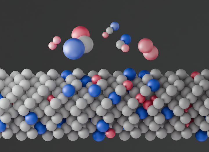
On the atomic scale, semiconductors are crystals made of different elements arranged in repeating lattice structures. Many semiconductors are made primarily of one element with a few others added to the mix in small quantities. There aren’t enough of these trace additives to cause a repeating pattern throughout the material, but how these atoms are arranged next to their immediate neighbors has long been a mystery. Do the rare ingredients just settle randomly among the predominant atoms during material synthesis, or do the atoms have preferred arrangements, a phenomenon seen in other materials called short-range order (SRO)? Until now, no microscopy or characterization technique could zoom in close enough, and with enough clarity, to examine tiny regions of the crystal structure and directly interpret the SRO.
“It’s an interesting scientific question because SRO dramatically changes the properties of a material. Our colleagues have predicted SRO theoretically in semiconductors, but this is the first time the individual structure of these SRO domains have been shown experimentally,” said co-lead author Andrew Minor, director of the National Center for Electron Microscopy at Berkeley Lab’s Molecular Foundry and a professor of Materials Science and Engineering at UC Berkeley.
The breakthrough moment came when first author Lilian Vogl, who was then a postdoctoral researcher in Minor’s lab, was studying a sample of germanium containing a small amount of tin and silicon using a powerful type of electron microscopy recently pioneered by the group called 4D-STEM. The initial results were too muddled to parse the faint signals from the electrons diffracting off the tin and silicon from the strong signals off the tidily arranged germanium, so she implemented an energy-filtering device on the system to improve contrast. When the next dataset started appearing on her monitor, she quickly realized there was a new kind of result. The faint signals were clearer, and repeating patterns emerged, indicating that the atoms have preferred order after all.
To validate her findings and learn what these patterns meant, Vogl collected more data with the energy-filtering 4D-STEM and used a pre-trained neural network to sort the diffraction images. The tool identified six recurring motifs representing particular atomic arrangements in the sample material, but the Berkeley Lab team still couldn’t determine the exact atomic structures that were generating the motifs. To interpret their experimental results, they turned to µ-Atoms collaborators at George Washington University led by co-lead author Tianshu Li, a professor of Civil and Environmental Engineering.
Li’s team generated a highly accurate and efficient machine-learning potential capable of modeling millions of atoms in the material’s structure, allowing Vogl to perform simulated 4D-STEM on different possible structural arrangements until she found matches for the motifs in the experimental data.
“It’s remarkable that modeling and experiment can work seamlessly to unravel SRO structural motifs for the first time,” said Li, whose team had previously predicted SRO and its impact and helped motivate the current study. “Proving SRO experimentally is not an easy task, let alone identifying its structural motifs. Signals from SRO can easily be obscured by defects or inherent movement of atoms at room temperature, and until now there was no clear way to separate them. This work represents the first step toward our broader goal.”
Read the full press release

