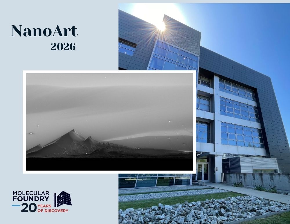
Have a very Nano New Year with the Molecular Foundry’s 2026 Calendar, featuring colorful submissions from the 2025 NanoArt Image Contest. The work behind these images comes from Foundry staff and users spanning all seven of the Foundry’s technical facilities.
Do you know which day is ‘National Nano Day’? Check the Foundry calendar!
Download and print your own copy.
About the 2026 Calendar
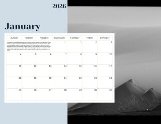
January
Submitted by Yashwanth Balaji and winner of the 2025 NanoArt contest, this image shows a cross-section of a silicon substrate. The striking pattern was formed during the cleaving process, where tiny microfractures created mountain-like structures. The scene evokes the likeness of a desert landscape: the silicon represents the endless expanse of sand, while the fractured ridge rises like a solitary mountain against the backdrop. SEM enables imaging of materials at the nanoscale. The contrast in the image varies depending on the material’s atomic weight and the orientation of its grains.

February
Submitted by Samuel Song (UC Berkeley). “Halloysite Heart”. A cluster of halloysite nanotubes upon a lacy carbon substrate resembling a human heart and biological tissue. Our project studies the geochemical factors governing the formation of mineral nanoparticles in volcanic soil in Rwanda. Chronic exposure to these mineral nanoparticles is believed to be trigger podoconiosis, a debilitating disease afflicting agricultural workers in the region.

March
Submitted by Shu Wang (UC Berkeley), in collaboration with Ali Javey. This is an optical microscope image of an array of crystals. They are grown on a very thin layer of a patterned array of metal (2 nm) and grown following the pattern. High refractive index makes it shine. This material is for higher efficiency light-emitting devices.

April
Submitted by Ambarneil Saha. You’re looking at stills from a virtual dark-field movie of an organic nanocrystal deteriorating due to radiolytic damage. These coherently diffracting domains disintegrate with remarkable fluidity, undulating with patterns of contrast that swell and recede like waves in a turbulent sea. This technique helps us (a) mechanistically understand and (b) mitigate radiation damage, the fundamental limit constraining all electron microscopy.
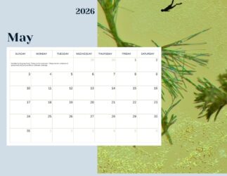
May
Submitted by Qingsong Zhang. “Diving into the crystal sea” – Charge transfer complexes for optoelectronic devices resemble an underwater landscape.
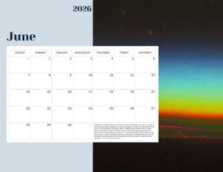
June
Submitted by Christina Boukouvala. “Sunset over a silicon nitride landscape”. This is an image of a broken silicon nitride grid taken with an optical microscope. The edge of the silicon nitride, which can be seen at the bottom of the image, refracts the light forming a rainbow, similar to a prism. Silicon nitride grids are custom made with very thin windows that support various fabricated nanostructures. The windows are only a few tens of nanometers thick and break easily; we need them to be thin in order to characterize the optical response of the fabricated nanostructures. By knowing the optical properties of the nanostructures we can then tailor their design for various applications, such as for chemical sensing.
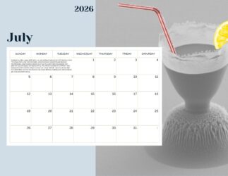
July
Submitted by Adam Legacy (HiRi Optics, Inc) and winning 6th place in the 2025 NanoArt contest. This image shows a tiny ‘nano lemonade’, a layered structure created through advanced microfabrication. A light-sensitive polymer sits on top of a custom high-index polymer, both patterned using lithography and plasma etching. The different materials etch at different rates, leaving behind this small disc-shaped structure with unique sidewalls. Improving the way light from optical fibers connects into photonic chips boosts efficiency, enabling faster internet speeds and more powerful AI training.

August
Submitted by Kate Reidy in collaboration with Kang’an Wang and Dana Bryne. “Nanofish Under the Sea”: This image shows stacked two-dimensional (2D) materials, slightly rotated to create reconstructed moiré patterns (that look like fish scales). The dark “eye” is a tiny bubble where the layers misaligned. Captured using dark-field transmission electron microscopy (TEM), to reveal nanoscale structure and domain boundaries. Stacking and twisting 2D materials allows us to tailor their electronic and optical properties. These insights could lead to faster, more energy-efficient computers, next-generation batteries, and new ways to harvest or store energy.
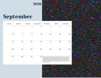
September
Submitted by Stephanie Ribet, winning 5th place in the 2025 NanoArt contest. This is a dark-field STEM image depicting self-assembled, polymer-grafted gold nanorods. The nanorods are false-colored based on their orientation to emphasize their alignment arising from interactions mediated by the grafted polymer chains. By integrating correlative resonant soft X-ray scattering data obtained at the Advanced Light Source with electron microscopy data collected at the Molecular Foundry, we aim to establish new approaches to quantitatively probe nanoscale ordering in soft and composite materials.

October
Submitted by Alexandre Bordas and winning 4th place in the 2025 NanoArt contest. Meet Jack-o-Lamella, a nanoscale sculpture crafted using a focused ion beam. This ScAlN sample was destined to uncover how local atomic arrangements can cause improved dielectric performance in devices. The thinning process to prepare this material for nanoscale analysis, however, left holes in the substrate and a spooky face was revealed. ScAlN is a promising dielectric material for next-generation electronics.

November
Submitted by Yen Jea Lee and winning 2nd place in the 2025 NanoArt contest. This image shows a nanostructure composed of peptoid molecules that arrange themselves into feather-like patterns. What may look like abstract art is in fact a chemical phenomenon at the molecular scale, where precise design enables matter to self-assemble with remarkable accuracy and beauty. Peptoid-based nanostructures that program molecular interactions can be used in future materials design to control both structure and function, while also enabling the creation of interfaces between biological and physical systems.
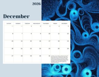
December
Submitted by Usama Choudhry in collaboration with Alexander Stibor, winning 3rd place in the 2025 NanoArt conest. Atomic terraces can be seen on a (110) surface of a tungsten crystal. Repeated thermal annealing can cause the steps to migrate across the sample surface and form these dramatic, whirl-pool like step bunches. The QSPLEEM microscope enables atomic-level imaging of surface layers, making it invaluable for characterizing magnetic and electronic properties in next-generation device materials.

