By Isha Nadig
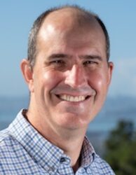
Paul Ashby is the Facility Director of the Foundry’s Imaging facility. His affinity for science emerged in grade school, watching the “Principles of Electrochemistry” series on the Los Angeles School District UHF broadcast channel. Later, during a game of Trivial Pursuit, he surprised his family, correctly answering a question on chemistry. During his PhD in Physical Chemistry at Harvard University, Ashby initially believed he would pursue teaching after graduation. However, an unexpected offer by the highly-regarded materials scientist, Miquel Salmeron, to begin a postdoc at the Molecular Foundry changed his plans. At the time, the Foundry was only an exciting idea. Ashby remarks, “Miquel laid out the blueprints of what came to be the first floor of the facility. In essence, he was laying out the vision of the Foundry as this interdisciplinary user facility to do nanoscience.”
As a postdoc, staff scientist, and now facility director, Ashby is energized by the collaborative atmosphere, the impact of nanoscience discovery, and, naturally, the beauty of the bay. At the Molecular Foundry, he is regularly exposed to a range of user projects and science, allowing him to fulfill his desire of teaching others while advancing scientific discovery. Ashby reflects, “it’s the variety of science that I value so much.” In addition to collaborating with users, Ashby enjoys occasional conversations with other colleagues over an espresso at ‘Café Cabrini’, the lounge space for the imaging and nanofabrication facilities. The Foundry is filled with interaction spaces and he notes, “lots of good ideas come from just sitting down and having a conversation.”
Beyond his impactful contribution to user projects, Ashby is motivated to uncover the fundamental physics which drives the assembly of soft materials from nanostructures. To achieve this, he uses Atomic Force Microscopy (AFM), one of the only nanoscale characterization tools able to operate in liquids and capture dynamic movement at high resolution. Ashby employs the AFMs at the Foundry to probe the energy landscapes of functional assemblies and elucidate their mechanical properties. His most valuable discovery for improving AFM time-resolution and scanning rate has been high-sensitivity cantilevers and new mechanics for high-speed scanning. High-speed scanning AFMs can have a major impact on the microelectronics industry when studying EUV resist materials. During EUV resist development, an etching process removes underlying material using an extremely basic solution, which causes the resist to swell. High-speed scanning AFM can capture this dynamic process in real-time – in corrosive liquid and at high resolution.
Interested in Becoming a Foundry User?
Join our collaborative, multidisciplinary environment.
Learn more >
As Ashby reflects on the Foundry’s past twenty years, he notes the significant progress Foundry scientists have made in controlling nanoscale matter, and the progress yet to be made. “We’ve made a huge leap forward in our ability to nanostructure materials, and not only to structure, but to predict the properties of these materials that we’re making.” The next step will be to predict the material structure from the desired properties. Fundamental research will be integral to achieving this. Ashby remarks, “basic science allows us to discover things we wouldn’t otherwise discover, which can have societal value as the ‘aha’ moments turn into the ‘oh wow, this is really impactful’.”

