By Claire Tsai
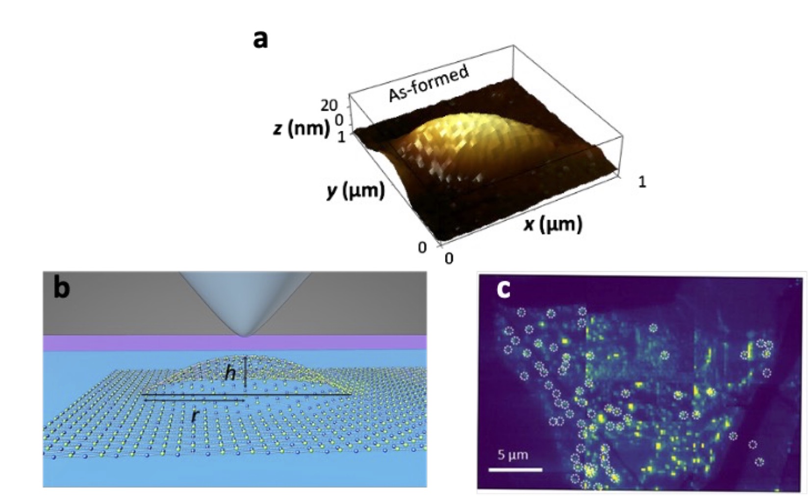
At the Molecular Foundry, what started as a microscopic mistake turned into an illuminating breakthrough. While carefully stacking atomically thin sheets of tungsten diselenide (WSe2), often used in semiconductors, postdoctoral researcher Junze Zhou noticed that the tiny air pockets trapped between layers unexpectedly began to glow. These “bubbles,” each only hundreds of nanometers wide, have become subjects of single-photon emitters, which release one photon at a time, a property prized for quantum communication and computing.
The bubbles form spontaneously, like trapped air pockets under stretched film, as uneven contact during the stacking of ultrathin WSe2 sheets on smooth surfaces causes bubble-like distortions, and are typically unwanted—often regarded as defects. “Nanobubbles first appeared during sample preparation and were randomly found in the sample. So at the beginning, we did not plan to study nanobubbles at all,” Zhou reports. A review of the literature pointed to earlier work by Thomas Darlington, a Scientific Engineering Associate in the Imaging Facility, who found that the strain within the nanobubbles could alter their electronic and optical properties, even enabling single-photon emission.
Traditional research on nanobubbles has often relied on glass lenses that focus and collect light from far above the sample, making it difficult to isolate the signal from a single nanobubble. To study and control individual bubbles at the nanoscale, Zhou devised an innovative dielectric near-field probe—a sharply tailored glass fiber that works as both a light source and detector. As a postdoc at the Foundry, Zhou has been developing this instrumentation to advance optics research on-site. “We now have a near-field lab dedicated to the scanning near-field optical microscope, but when I arrived, we didn’t have it. What we had at that time was a scanning station, and I started to build the optics around it,” Zhou recalls.
Zhou’s pioneering usage of a dielectric near-field probe allowed the team to modulate the strain and emission—something that has not been possible with other methods for creating single-photon emitters—with remarkable precision at the nanoscale at room temperature by directing light down to the tip and collecting the returning signal. To achieve this, the team scanned the probe across the sample to map the topography of the bubbles, and then positioned the tip on a single bubble and pushed down, allowing the local strain modulator, the excitation source, and the detection to all be integrated. Darlington explains, “These dielectric field probes are, in principle, way more powerful than standard far-field optics because you don’t have light coming from everywhere—you can localize it right at the surface.” As they press, the material is stretched right under the tip, changing the energy of the light that comes out, so the glow from that spot shifts toward red. “Because you’re creating increased strain, the energy band gap becomes even smaller, causing the red-shifted emission” Dr. Alexander Weber-Bargioni, a staff scientist at the Foundry elaborates. With this new device, what started as an annoyance to most scientists working on 2-D materials has become the most broadly and reliably tunable photon source, which is critical not only for quantum information systems, but other advanced sensing approaches. The team’s results were published in Advanced Materials.
The team also found that a bubble’s aspect ratio—its height compared to its radius—plays a central role in its formation and luminescence. The elastic energy that forms a bubble depends not on its size but on that ratio, offering clues to how such nanoscale features might be deliberately engineered rather than left to chance. To better understand the mechanical forces at play, Darlington performed a series of simulated calculations to model how the probe interacts with the bubble. “From broad analysis, you can understand what the force must be based on how the tip is being pushed down and how the bubble pushes up,” Darlington reports. “You have some force pushing up and then a bigger, but narrower, force pushing down. You feed that force into the plate equations and ask: what kind of strain distribution must result from that?”
Interested in Becoming a Foundry User?
Join our collaborative, multidisciplinary environment.
Learn more >
This discovery was made possible due to the Foundry’s unique environment. “I feel fortunate to have access to tools and help develop them as a post-doctorate at the Foundry,” Zhou says. As a user facility, the Molecular Foundry thrives on shared expertise and open collaboration. “The Foundry has traditionally worked in a very collaborative manner on all these nanoscale materials and so we have developed an enormous toolbox of different characterization techniques that enable us to measure material properties at the critical length and time scales where things really are happening,” Weber-Bargioni added.
Looking ahead, the team hopes to selectively finetune the nanobubbles’ photon emissions and their energy via precise strain engineering. “The next step is to use these stretching approaches either to engineer the single‑photon sources or to design devices that harness specific strain states,” Darlington explains. Such tunable photon emitters allow for the emission of identical photons, a critical requirement for advancing quantum technologies. In photonic quantum computing, for example, these identical photons can be used to link their states, forming quantum entanglement—the foundation for secure communication and powerful quantum logic operations. “If you can control emissions, that has a huge impact technologically on the ability to make a photonic‑based quantum computer. It’s one of the keys to advancing quantum technologies,” Weber-Bargioni notes.

