Scientific Achievement
A team of users and staff working at the Molecular Foundry have created a thermal imaging technique that can “see” how temperature changes from point to point inside the smallest electronic circuits.
Significance and Impact
Modern microelectronic circuits contain billions of nanometer-scale transistors, each generating tiny amounts of heat that collectively can compromise the performance of the device.
Research Details
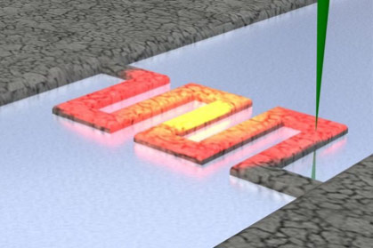
- Electron microscopes can image structures with nanometer resolution.
- As the probing electrons pass through the sample they excite collective charge oscillations called plasmons.
- The energy required to excite the plasmons depends on a nanowire’s density, which is directly related to temperature.
- Researchers developed a new technique called plasmon energy expansion thermometry, or PEET, that enables the measurement of local temperature with 3-5K precision and 5nm spatial resolution, a 100 fold resolution improvement.
- It’s the only technique that correlates atomically resolved structure to a device’s thermal characteristics.

