Scientific Achievement
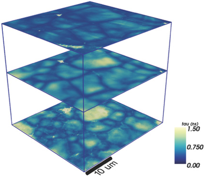
A team of Molecular Foundry scientists and users have developed a way to use optical microscopy to map thin-film solar cells in 3-D as they absorb photons.
Significance and Impact
The method images optoelectronic dynamics in materials at the micron scale to see individual grain boundaries, substrate interfaces, and other internal obstacles that impacts a solar cell’s efficiency.
Research Details
- A solar cell’s subsurface realm—where much of the energy-conversion action happens—has been inaccessible to real-time, nondestructive imaging
- Staff and industry users from PLANT PV modified a technique from biology called two-photon microscopy.
- Using two highly focused laser beams of infrared photons that penetrate inside the photovoltaic material, they can excite and track electrons to map the material’s optoelectronic properties.
- Users from NREL came to use the new method to study CdTe solar cells.

