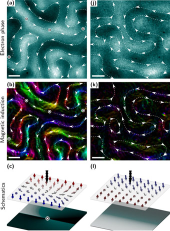
A team of Foundry staff and users has confirmed a special property known as “chirality” – which potentially could be exploited to transmit and store data in a new way – in nanometers-thick samples of multilayer materials that have a disordered structure.
While most electronic devices rely on the flow of electrons’ charge, the scientific community is feverishly searching for new ways to revolutionize electronics by designing materials and methods to control other inherent electron traits, such as their orbits around atoms and their spin, which can be thought of as a compass needle tuned to face in different directions.
These properties, scientists hope, can enable faster, smaller, and more reliable data storage by facilitating spintronics – one facet of which is the use of spin current to manipulate domains and domain walls. Spintronics-driven devices could generate less heat and require less power than conventional devices.
In the latest study, the researchers confirmed a chirality, or handedness, in the transition regions – called domain walls – between neighboring magnetic domains that have opposite spins.
Experiments revealed a dominant chirality in the magnetic properties of these domain walls that could possibly be flipped to its opposite. Such a flipping mechanism is a critical enabling technology for spintronics and variant fields of research that are based on the electron’s spin property.
The science team worked to identify the right thickness, concentration, and layering of elements, and other factors to optimize this chiral effect.
The research team enlisted a unique, high-resolution electron microscopy technique at the Molecular Foundry, and conducted the experiments in a so-called Lorentz observation mode to image the magnetic properties of the material samples. The Lorentz microscopy technique employed at the Foundry’s National Center for Electron Microscopy provided the tens-of-nanometers resolution required to resolve the magnetic domain properties known as spin textures.

