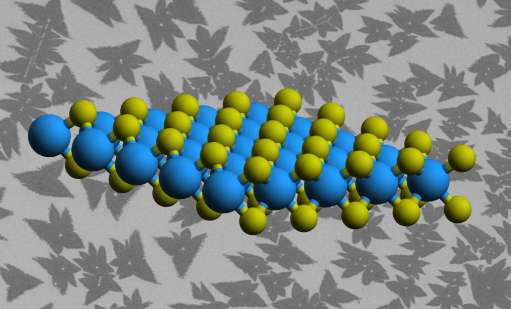
Nothing is perfect, or so the saying goes, and that’s not always a bad thing. In a study by Foundry staff and users, the research team learned how nanoscale defects can enhance the properties of an ultrathin, so-called 2D material.
They combined a toolbox of techniques to home in on natural, nanoscale defects formed in the manufacture of tiny flakes of a monolayer material known as tungsten disulfide (WS2) and measured their electronic effects in detail not possible before.
Tungsten disulfide is a well-studied 2D material that, like other 2D materials of its kind, exhibits special properties because of its atomic thinness. It is particularly well-known for its efficiency in absorbing and emitting light, and it is a semiconductor.
Members of this family of 2D materials could serve as high-efficiency computer transistors and as other electronics components, and they also are prime candidates for use in ultrathin, high-efficiency solar cells and LED lighting, as well as in quantum computers.
These 2D materials could also be incorporated in new forms of memory storage and data transfer, such as spintronics and valleytronics, that would revolutionize electronics by making use of materials in new ways to make smaller and more efficient devices.
The latest result marks the first comprehensive study at the Lab’s Advanced Light Source (ALS) involving a technique called nanoARPES, which researchers enlisted to probe the 2D samples with X-rays. The X-rays knocked out electrons in the sample, allowing researchers to measure their direction and energy. This revealed nanoscale defects and how the electrons interact with each other.
The team also enlisted a technique known as XPS (X-ray photoelectron spectroscopy) to study the chemical makeup of a sample at very small scales; a form of AFM (atomic force microscopy) to view structural details approaching the atomic scale; and a combined form of optical spectroscopy (Raman/photoluminescence spectroscopy) to study how light interacts with the electrons at microscope scales.
Adam Schwartzberg, a staff scientist at the Molecular Foundry who served as a co-lead in the study, said, “It took a combination of multiple types of techniques to pin down what’s really going on.” He added, “Now that we know what defects we have and what effect they have on the properties of the material, we can use this information to reduce or eliminate defects – or if you want the defect, it gives us a way of knowing where the defects are,” and provides fresh insight about how to propagate and amplify the defects in the sample-production process.
While the concentration of edge defects in the WS2 flakes was generally known before the latest study, Schwartzberg said that their effects on materials performance hadn’t previously been studied in such a comprehensive and detailed way.
Researchers learned that a 10 percent deficiency in sulfur atoms was associated with the defective edge regions of the samples compared to other regions, and they identified a slighter, 3 percent sulfur deficiency toward the center of the flakes. Researchers also noted a change in the electronic structure and higher abundance of freely moving electrical charge-carriers associated with the high-defect edge areas.
For this study, the defects were due to the sample-growth process. Future nanoARPES studies will focus on samples with defects that are induced through chemical processing or other treatments. Researchers hope to control the amount and kinds of atoms that are affected, and the locations where these defects are concentrated in the flakes.
Such tiny tweaks could be important for processes like catalysis, which is used to enhance and accelerate many important industrial chemical production processes, and to explore quantum processes that rely on the production of individual particles that serve as information carriers in electronics.

