By Brooke Kuei

Optoelectronics – technology that gives off, detects, or controls light – are used everywhere in modern electronics and include devices such as light-emitting diodes (LEDs) and solar cells. Within these devices, the movement of excitons (pairs of negative electrons and positive holes) determines how well the device performs.
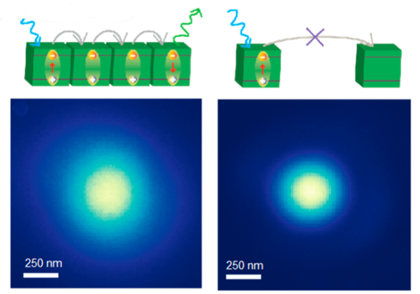
Until now, the distance that excitons could travel in conventional optoelectronic systems was around 30-70 nanometers, and there was no way to directly image how the excitons move. In a study recently published in ACS Nano, a team of Foundry researchers designed and made a nanocrystal system in which excitons can move a record distance of 200 nanometers, an order of magnitude larger than what was previously possible. They also built a custom microscope that can directly image the movement of excitons.
“The scientific achievement is that we found an artificial system in which an exciton hops from crystal to crystal over very long distances, ten times farther than previously achieved,” said Alex Weber-Bargioni, facility director of the Imaging and Manipulation of Nanostructures Facility at the Molecular Foundry and principal investigator of the study. “Then there’s the technical achievement – we are able to directly image the movement of the excitons to better understand their behavior.”
Their system consists of tiny crystals of perovskites, a class of crystals that are emerging as promising materials for optoelectronic devices.
“Perovskite nanocrystals form in a cubic shape, which makes them easy to pack together,” explained Monica Lorenzon, a post-doctoral researcher at the Foundry and an author of this work. “But they do not naturally do this over long distances.” Lorenzon described how her colleague Erika Penzo, first author of the paper, coated a silicon surface with a polymer containing chemical groups that the perovskite nanocrystals would attach to, forming a single layer of perovskite nanocrystals tightly packed together. This surface engineering process resulted in a nanocrystal system in which excitons could move from crystal to crystal over very long distances.
This system provided the researchers with a useful case study for looking at how excitons move, or diffuse, in more depth. “In optoelectronics, whether you are converting light to electricity or vice versa, you want to be able to tune and control the diffusion of excitons because they are the mediator of the light and the electronics.” said Weber-Bargioni. “So understanding how far and how fast excitons move is very useful.”
In the past, exciton movement was measured by adding defects, imperfections in a crystal that trap excitons. Researchers could track the movement of excitons indirectly by comparing samples with different amounts of defects. “But our system is much more direct,” explained Lorenzon. “We can actually visualize the exciton movement by directly imaging it with a custom-built microscope. This method also results in more accurate measurements, compared to the range of diffusion lengths that can be measured the indirect way.”
The basic principle of the microscope is that a laser is used to excite (transfer energy to) the material, resulting in an excited spot. As this energy is released, the photoluminescence (light given off by the material) at the same location will be a broader spot, like a drop of water on a paper towel that expands outwards over time. By comparing the excited spot to the photoluminescence spot, the average distance that excitons move can be measured, resulting in the record 200 nanometer diffusion length. “We hit the sample with a laser beam and if we filter out the laser light and we look at the photoluminescence light, we get a much broader spot – that is the excitons diffusing across the sample,” explained Lorenzon.
By adding time resolution, the microscope is also able to look at the dynamics of the excitons, and it was found that they first diffuse quickly and then slow down. This improved understanding of how excitons move can help enhance the performances of optoelectronic devices, where it is useful to tune exciton diffusion lengths for different applications, such as having long diffusion lengths in solar cells and short diffusion lengths in LEDs.
In a follow-up to this study, the researchers explored different methods (plasma vs thermal) for adding a thin, protective layer to the perovskite nanocrystals. Because this protective layer allows the nanocrystals to live for a longer time, the excitons can travel farther distances, which resulted in an even longer exciton diffusion length of 480 nanometers.
The custom microscope was also improved to include energy resolution. This revealed that energy stays the same as excitons move through the sample coated via the plasma process, whereas energy is decreased as excitons get trapped in defects and large crystals formed by melted nanocrystals in the sample coated via the thermal process. This work was recently accepted in Advanced Optical Materials.
Moving forward, the researchers are interested in looking at different classes of materials and different types of exciton diffusion using their microscope. They are also looking towards investigating whether the movement of excitons can be coherent, or move in sync with each other.

