Have a very Nano New Year with the Molecular Foundry’s 2023 Calendar, featuring colorful submissions from the 2022 NanoArt Image Contest. The work behind these images comes from Foundry staff and users spanning all seven of the Foundry’s technical facilities.
Do you know which day is ‘DNA Day’? Check the Foundry calendar!
Download and print your own copy.
About the 2023 Calendar
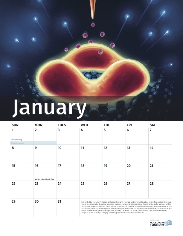
January
Submitted by Foundry Postdoctoral Researcher John Thomas, and winning 6th place in the NanoArt contest, this image is a schematic depicting tunneling electron-induced photon emission from a single sulfur vacancy within monolayer tungsten disulfide. The scanning tunneling microscope is capable of resolving photons emitted at the atomic scale, due to tunneling-induced luminescence and is used to observe quanrum interactions at the atomic scale. The work was performed by Bruno Schuler, Katherine Cochrane, John Thomas, and Alexander Weber- Bargioni in the Foundry’s Imaging and Manipulation of Nanostructures facility using the Createc Low Temperature STM/AFM.
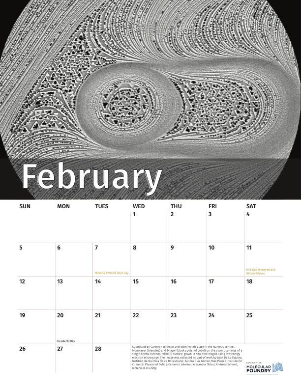
February
Submitted by Cameron Johnson and winning 4th place in the NanoArt contest. Monolayer (triangles) and bilayer (black spots) of cobalt on the atomic terraces of a single crystal ruthenium(1000) surface, grown in situ and imaged using low energy electron microscopy. The image was collected as part of work by Juan De La Figuera, Instituto de Química Física Rocasolano; Sandra Ruiz Gomez, Max Planck Institute for Chemical Physics of Solids; Cameron Johnson; Alexander Stibor, Andreas Schmid, Molecular Foundry using the qSPLEEM.
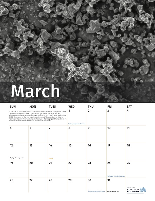
March
Submitted by Vittoria Tommasini. Growth of Transition Metal Dichalcogenides (TMDs). TMDs have interesting optical properties, such as optical switching and fast photodetecting, because the excitons are confined to one atomic layer, making them highly dependent on their surrounding environment. The work done by Vittoria Tommasini, Fabrizio Riminucci, Antonio Rossi used the Imaging and Manipulation of Nanostructures facility as well as the Nanofabrication facility.
April
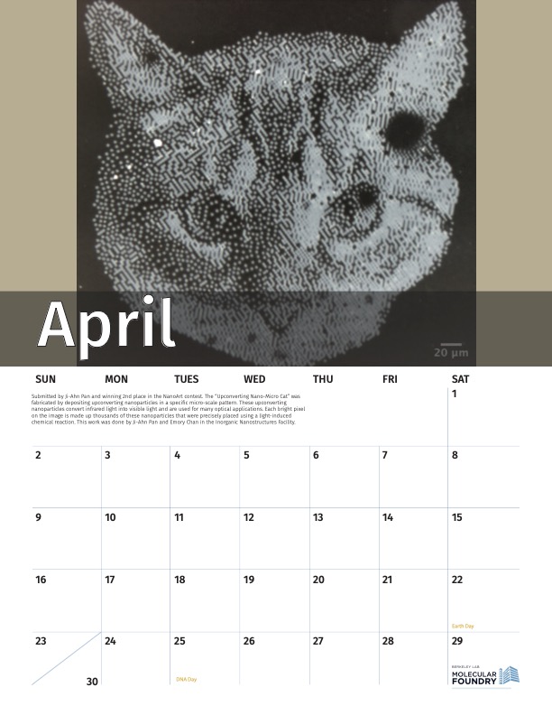
Submitted by Ji-Ahn Pan and winning 2nd place in the NanoArt contest. The “Upconverting Nano-Micro Cat” was fabricated by depositing upconverting nanoparticles in a specific micro-scale pattern. These upconverting nanoparticles convert infrared light into visible light and are used for many optical applications. Each bright pixel on the image is made up thousands of these nanoparticles that were precisely placed using a light-induced chemical reaction. This work was done by Ji-Ahn Pan and Emory Chan in the Inorganic Nanostructures Facility and made use of several instruments including the home-built photo-lithography station, optical microscope, Schlenk line synthesis, and spincoater.

May
Submitted by Stephanie Ribet. The focused ion beam (FIB) can be used to pattern phase and amplitude plates which are used for beam modification in the STEM. As illustrated here, the flexibility of the FIB allows for fabrication of intricate and complex apertures. Beam modification in a STEM opens the door for novel characterization of materials at nano to angstrom scale. The image was created at NCEM as part of work done by Stephanie Ribet, Northwestern University; John Turner, NCEM; Steven Zeltmann, UC Berkeley; Colin Ophus, NCEM using the FIB Helios G4.

June
Submitted by Beihang Yu. This is a surface contrast pattern created on silicon substrates by using electron beam lithography to pattern a polymer brush monolayer that passivates the surface. As a result we are able to have the DNA origami selectively lands in between the polymer brush lines. The research team is developing a workflow that combines the accuracy of top-town lithography and the precision of biomolecular assemblies. This will bring us the opportunity to do bio-templated large-area 2D nanopatterning with precision down to 1 nm. The image was created using the Imaging and Manipulation of Nanostructures facility and Nanofabrication facility as part of work by Beihang Yu (Molecular Foundry, Berkeley Lab), and Scott Dhuey, Boyce Chang, Whitney Loo, Ricardo Ruiz using several tools including electron beam lithography, plasma etcher, and atomic force microscopy.

July
Submitted by Steven Zeltmann, this image won 3rd place in the NanoArt contest. This is a simulation of a large-angle converged beam electron diffraction experiment performed on a silicon crystal. The web of criss-crossing lines that run through the pattern carry detailed information about the structure and symmetry of the crystal. Researchers can use these simulations to help determine the precise structure of nanomaterials The image was created at NCEM as part of work by Steven Zeltmann, UC Berkeley using the py4DSTEM package created by Ben Savitzky, Colin Ophus, and others, at NCEM.

August
Submitted by Yael Tsarfati. An orientation map of a semiconducting polymer’s thin film. The lines represent the local polymer chains orientations. The data is a visualization that is created based on diffraction patterns that are collected in an electron microscope in a technique called 4D-STEM. Color indicates chain direction and the intensity is correlated to diffraction intensity. Work by Dr. Yael Tsarfati & Dr. Luke Balhorn using the TitanX microscope.
September
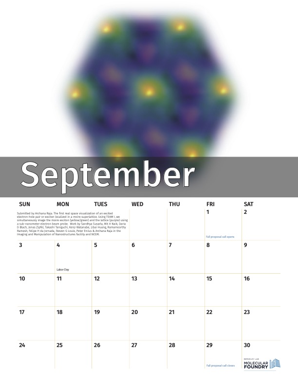
Submitted by Archana Raja. The first real space visualization of an excited electron-hole pair or exciton localized in a moire superlattice. Using TEAM I, we simultaneously image the moire exciton (yellow/green) and the lattice (purple) using a sub-nanometer electron beam probe. Work by Sandhya Susarla, Mit H Naik, Daria D Blach, Jonas Zipfel, Takashi Taniguchi, Kenji Watanabe, Libai Huang, Ramamoorthy Ramesh, Felipe H da Jornada, Steven G Louie, Peter Ercius & Archana Raja in the Imaging and Manipulation of Nanostructures facility and NCEM.
October
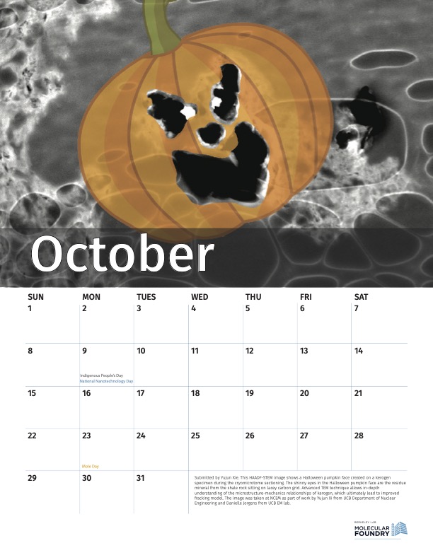
Submitted by Yujun Xie. This HAADF-STEM image shows a Halloween pumpkin face created on a kerogen specimen during the cryomicrotome sectioning. The shinny eyes in the Halloween pumpkin face are the residue mineral from the shale rock sitting on lacey carbon grid. Advanced TEM technique allows in-depth understanding of the microstructure-mechanics relationships of kerogen, which ultimately lead to improved fracking model. The image was taken at NCEM as part of work by Yujun Xi from UCB Department of Nuclear Engineering and Danielle Jorgens from UCB EM lab using the FEI ThemIS microscope.

November
Submitted by Min Chen. This is the lameallar structure of polymer PS-b-PEO STEM image. The TEAM 1 microscope at NCEM provides a detailed microstructure to help researchers better understand the phase separation of the coploymer. The image was collected by Min Chen at NCEM using materials from Prof. Nitashi Balsara’s research group and the TEAM 1 microscope.
December
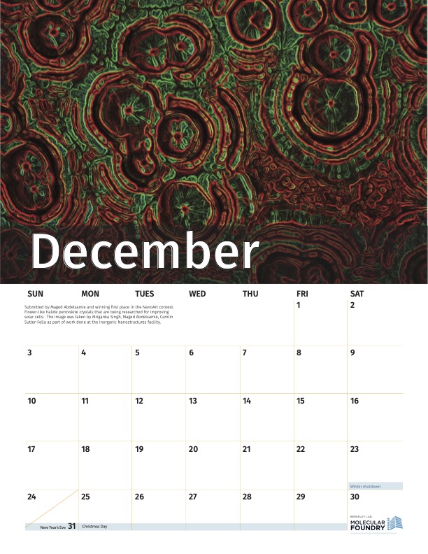
Submitted by Maged Abdelsamie and winning first place in the NanoArt contest. Flower-like halide perovskite crystals that are being researched for improving solar cells. The image was taken by Mriganka Singh, Maged Abdelsamie, and Carolin Sutter-Fella as part of work done at the Inorganic Nanostructures facility.

