Seminar Date: Tuesday, February 21, 2023
Time: 11:00 am
Location: 67-3111 & Zoom
Talk Title: Electronic-Structure Engineering through Atomic-Scale Strain Control in Complex Oxide Heterostructures
Zoom recording available for 30 days after the seminar. Passcode: +C6m0D#.

Bio:
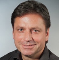
Prof. Dr. Peter A. van Aken leads the Stuttgart Center for Electron Microscopy (StEM), adding exceptional strength to the analytical capabilities of the Max Planck Institute for Solid State Research. StEM possesses outstanding expertise in scanning and transmission electron microscopy (TEM), focused ion-beam applications, and methodology development. Prof. van Aken’s research focuses on the atomic-scale characterization of interfaces, functional complex oxide hetero-structures, strained semiconductors, of optical properties of nanostructured thin films and plasmonic-active nanostructures, nanoparticles and nanomaterials, as well as of molecules on 2D materials. He uses and further develops the advanced scanning TEM techniques electron energy-loss spectroscopy, energy-dispersive X-ray spectroscopy, in-line electron holography, in-situ TEM methods, strain mapping, quantitative high-resolution TEM analysis, different quantitative electron diffraction techniques, image processing and simulation, and 4D-STEM, electron ptychography and tomography. Prof. van Aken’s research mission is the advancement of the in-depth microscopic understanding of materials with respect to their functionalities and structure–property relationships.

