By Matt Lundy

The harnessing of solar power is a critical pillar in the next generation of electrical infrastructure, and it will require large-scale manufacture and deployment of photovoltaic (PV) panels. A relatively new class of materials, organic–inorganic halide perovskites, offers an alternative to silicon for PV power generation. These materials can either work in combination with silicon in tandem PVs to increase efficiency, or they can operate on their own.
A team of international researchers led by Rui Wang, Yang Yang, Mohammad Khaja Nazeeruddin, and Jingjing Xue and including staff at the Molecular Foundry and Advanced Light Source (ALS) at Lawrence Berkeley National Laboratory (LBL) experimented with halide perovskites in a recently published Nature study. Halide perovskites are prime candidates for research because they offer a range of benefits when compared with their traditional counterpart. Benefits of perovskites include being a film up to 1000 times thinner than silicon, absorbing incoming solar irradiation more efficiently, and having a better matched bandgap for the solar spectrum. Perovskite thin film fabrication also offers lower cost processes when compared to silicon wafer generation, but more research, such as this study, needs to be done to capitalize on that potential.
Black-phase formamidinium lead iodide perovskite (FAPbI3) is one of the most promising halide perovskite candidates for PV applications. One challenge to overcome, however, is the existence of polytypes, which are different configurations of the same atoms, called black and yellow phases for this material. At room temperature, the yellow phase is the most stable. But the yellow film is relatively transparent to the solar spectrum and consequently results in solar energy conversion losses. In contrast, the black-phase formamidinium lead iodide absorbs most of the solar spectrum. But the black phase is energetically unfavorable and is therefore not normally stable at room temperature. As a consequence the photoactive black phase is hampered by its conversion to the non-photoactive yellow phase. To counteract this, the research team has developed a new method of perovskite crystallization which reliably suppresses yellow phase formation, leading to improved photovoltaic performance.
The team made use of specially designed and developed capabilities at the ALS which allowed for real-time monitoring of the perovskite’s crystallization. This crystallization process occurs rapidly and is hard to follow in detail. To account for this, the ALS’s tool, consisting of a spin coater operated in the hutch of and attached to the micro X-ray diffraction beamline 12.3.2, was uniquely developed to be able to track fast occurring crystallization processes.
“People did not have off-the-shelf characterization tools to follow these fast changes in crystal structure or optical properties. So, this is how we came into the story,” said Carolin Sutter-Fella, a staff scientist at the Foundry’s Inorganic Nanostructures Facility.
The development of the spin coater with heating capability at the beamline was crucial for the study’s in-situ measurements to provide novel insights during the perovskite’s initial nucleation. The spin coater development was started by Sutter-Fella, and ALS engineer Jonathan Slack facilitated successful design and implementation, including sophisticated technical solutions required for the experiments.
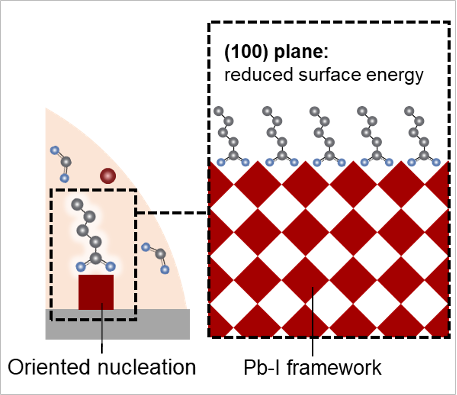
With the specialized tools, including the ALS’s spin coater and the Foundry’s optical spectroscopy setups, high time-resolution and in-situ measurements were possible. Researchers were able to both monitor crystal phase changes and study the influence of additives on the crystallization pathway. They found great success through the introduction of additives such as pentanamidine hydrochloride (PAD) to the starting materials. By adding PAD, nucleation of the perovskite was altered such that the yellow and other intermediate phases were suppressed, allowing black phase to become the material’s single phase.
Interested in Becoming a Foundry User?
Join our collaborative, multidisciplinary environment.
Learn more >
It was found that PAD strongly interacts with the lead iodide framework. This interaction led to a decrease in surface energy for one specific (100) plane driving the preferential formation of (100) oriented black-phase FAPbI3. In the absence of PAD, multiple phases including the yellow phase accompanied the black phase evolution.
With PAD added, the perovskite growth was not only well oriented, and thus higher quality, but also slowed down as revealed by in-situ measurements allowing for more synthesis control. These results were in stark contrast to the reference growth of perovskite without any additives, which featured essentially random orientation of the crystal planes.
The additive strategy was applied to different fabrication processes and was found to be universally applicable as a strategy to achieve stable black-phase perovskite. “The interesting thing here is that there is a unifying mechanism that can explain how you preferentially grow the photoactive black phase,” said Sutter-Fella.
This research made use of significant crossover between Foundry and ALS user capabilities. The spin coater attachment is located at the ALS beamline 12.3.2, and it is supported by Sutter-Fella’s research team, the beamline scientist Nobumichi Tamura, and the ALS’s engineering and beamline control teams. Experiment preparation and complementary in-situ measurements were performed at the Foundry. This study highlights the benefits of the proximity and partnership between the Foundry and ALS.
In looking at future steps, Sutter-Fella hopes to expand these advanced characterization capabilities to industry-relevant and scalable processes. “The majority of research groups are currently using spin coating for these perovskite materials, but that is not an industry relevant process. So, one thing I want to do next is to start the multimodal, in-situ characterization on large area scalable techniques, for example blade coating,” said Sutter-Fella.
She also talked about steps beyond the current material case. “Ideally, I want to broaden this to other material classes, not just perovskites, because many people use a solution process to fabricate a thin film. One other big field is polymers: organic semiconductors for example… I’m really looking forward to applying this state-of-the-art capability to other functional materials.”

