Adapted from this Berkeley Lab article

Cryogenic electron microscopy, or cryoEM for short, is another critical research tool that the Lab is developing. In the last five years, with the growing interest in quantum computing and in superconducting materials, the need to examine materials that only exist or operate at low temperatures, has exploded. But today’s electron microscopes, which are optimized to function at room temperature, don’t work well for examining many temperature-sensitive materials. Image resolution of these materials is poor, partly due to significant drift that occurs when “cold” materials are in room temperature environments. In addition, many materials change their structure at room temperature.
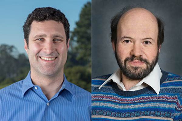
Andy Minor, facility director of the Foundry’s National Center for Electron Microscopy (NCEM) , said, “Having your sample drift around while you’re trying to examine them at atomic resolution is a problem. Fundamentally, having a 300 degree difference in temperature between the sample and the instrument is just too limiting.”
Other approaches to reduce the problem of drift due to thermal expansion, such as putting a low temperature stick into a room temperature microscope, have been explored, but they don’t work well.
CryoEM is an approach that has been explored since the 1960s. Lab scientist Robert Glaeser has been recognized for his groundbreaking work in cryoEM research. The biological science community relies on averaging (combining multiple images) to improve resolution at cryogenic temperatures using room temperature microscopes, but this approach is not available for materials that are unique and can’t be averaged. Therefore, new approaches to cryoEM could significantly open up the range of materials that can be explored. Another advantage of the cryoEM approach is that the electron source can be improved; colder sources make higher quality beams, but they are a challenge for room temperature microscopes.
Andy and his team have been working on building a new type of cryoEM instrument since 2019. That year, Andy, fellow Lab scientist Peter Denes, and Cornell University scientist David Muller organized a workshop to explore the many things that could be achieved with such a microscope. Following the workshop, the team published a paper and successfully pitched the DOE for funds to conduct initial development.
In the last three years, a team led by Peter and Andy, leveraging the expertise of the Berkeley Center for Magnet Technology, have built significant components of a cryoEM: a lens that is stable and a superconducting tip through which to shoot electron beams at the sample. But a cryoEM has hundreds of lenses. And it also requires detectors and software. Putting all these components together, first into a prototype low-voltage system, and then testing the instrument’s performance, will be an expensive proposition.
Interested in Becoming a Foundry User?
Join our collaborative, multidisciplinary environment.
Learn more >
The good news is that there is strong demand for better electron microscopes. “Everyone who has a modern electron microscope would like a better one — semiconductor companies, pharmaceutical companies, materials researchers, and biologists,” said Andy.
“The impact of an ultrastable and ultracold cryoEM could be very large,” he continued. “Understanding the structure of materials at atomic scales is critical, and cryoEM would open so many doors, whether for developing new battery materials or quantum computers or biological materials. It will be interesting to see what people do with it,” he said.
Read the full press release

