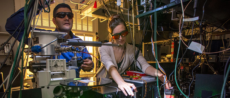
This Facility’s staff applies and develops techniques to characterize and manipulate a broad variety of nanostructures, from hard to very soft matter, including liquid structures. Imaging methods span electron, optical and scanning probe microscopy, including combined electron-scanning probe and near-field optical-scanning probe instruments. In situ experiments are performed by combining microscopy with manipulation tools and controlled environments. Nanostructure characterization tools include advanced optical spectro-microscopy (linear, non-linear, tip-enhanced and pump-probe) and Auger and x-ray photoemission for surface analysis. Take a Virtual Tour.
Highlighted Research Programs
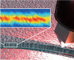
Mapping Chemical and Optoelectronic Properties at Length Scales that Matter
Advanced nano-optical imaging and spectroscopy capabilities are being developed that push the limits of resolution and sensitivity to the single-molecule level. The campanile near-field tip shown here, allows the mapping of local chemical, optoelectronic, morphological and dynamical information in novel nanostructures, ultimately correlating the mesoscale interactions of these properties with material functionality.
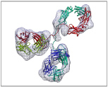
Single-Protein
Cryo-EM Tomography
3D imaging of a single protein has been achieved through a new technique called individual-particle electron tomography (IPET). Images of an individual IgG antibody with 1.4nm resolution have been demonstrated. IPET enables researchers to observe the dynamics and fluctuation characteristics of single antibodies in physiological environments.
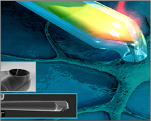
Encased Cantilevers for Atomic Force Microscopy in Liquids
Encased cantilevers are ultra-sensitive AFM probes optimized for nanoscale biomedical imaging and investigation of materials and interfacial processes that occur in liquids. While the sample remains in a liquid environment, a hydrophobic encasement allows the cantilever to stay dry, resulting in less damping and increased force sensitivity by more than an order of magnitude.
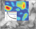
Depth-Resolved Probing and Lifetime Imaging of Carrier Dynamics in PV Materials
Nonlinear optical capabilities are being developed to map properties, such as carrier lifetimes in three dimensions, in novel materials and real devices. These techniques allow researchers to probe heterogeneity in dynamics in subsurface structures (e.g., buried interfaces and defects), in order to better understand carrier dynamics and improve the performance of (opto)electronic devices.

