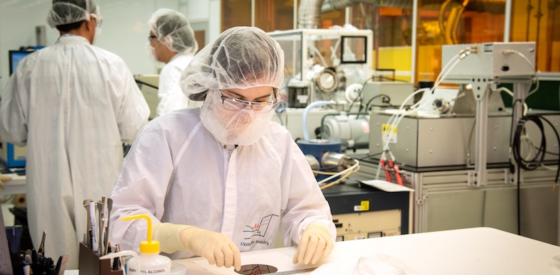
Our facility strives to gain insight into fundamental nanofabrication processes, as well as the generation of structures that control light, electron, or energy flow, and how those, and other, nanoscale structures interact with light on ultrafast time scales.
Highlighted Research Programs
Measuring Plasmonic Structures
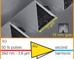
High yield and performance optical transformers are fabricated by nanoimprint lithography for near-field probe and ultra-resolution sub-surface imaging (a). The new ultrafast laser lab uses second harmonic generation imaging to probe the plasmonic enhancement frequency response of these and other photonic and plasmonic structures.
Integrating Multi-Modal Optical Devices
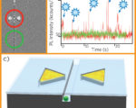
A new analytical device has been developed that uses a fluidic channel to deliver a specific target to a plasmonic hot spot created by a nanoantenna (c). The fluorescence of single quantum dots flowing in the channel can be observed when focusing excitation onto the antenna (red circle (a) and trace (b)), but not when focusing on the channel alone (green circle (a) and trace (b)).
Single Digit Nanofabrication
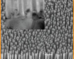
Cryogenic plasma etching and block co-polymer lithography has been used to create a 10 nm silicon nanowire forest. Transmission electron microscopy shows 60 nm deep wires. Moire fringes in the individual wired (inset) demonstrate crystallity.
Quantum Control of Exciton Flow
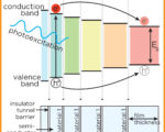
By making films at thicknesses below the Bohr-exciton radius of a semiconductor (~3-30 nm), it is possible to tune the band gap of that material. By placing a thin, wide band-gap material between such layers and carefully controlling each layer thickness, it will be possible to energetically channel excitons from the source of generation to the location of work to be done.

