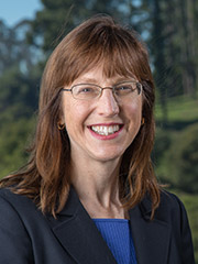
Scientific Engineer, NCEM
510.486.4324
Biography
Karen Bustillo obtained her Ph.D in Materials Science and Engineering from the University of California, Berkeley. Her doctoral work focused on the optical properties of semiconductor nanoparticles. Her M.S. degree research involved using solid state NMR to study bonding configurations in amorphous carbon. In addition to transmission electron microscopy, Karen has expertise in Raman, photoluminescence, FTIR, and UVVis spectroscopies, as well as a variety of conventional semiconductor processes.
Research Interests
Karen is the staff member overseeing the Thermo Fisher TitanX and ThemIS microscopes, and she can assist with the TEAM I. In addition to conventional TEM methods, she is available to train users in the following techniques:
- Insitu experiments including cryo, heating, mechanical testing, Protochips platform (heating and biasing), liquid cell, and gas cell.
- EDS and EDS tomography
- STEM tomography
- EELS and EFTEM
- 4D-STEM for strain mapping, diffraction mapping, precession diffraction and fluctuation microscopy
- MicroED
- TEM Analysis tools
Dr. Bustillo’s research interests include imaging of soft materials using advanced techniques such as scanning nanobeam diffraction. She pursues characterization of nanostructures using the EDS capabilities of the TEM especially with respect to elemental quantification and data analysis. In the past, her research focused on plasmonic nanoparticles: nonequilibrium phases, low-loss plasmon mapping, and structure. She is also interested in technique development in the TEM.


