December 2022
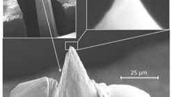
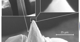
To Make a Better Electron Microscope, Go Straight to the Electron Source
December 2022
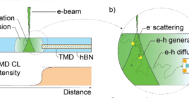
A Sharper, Deeper View into Semiconductor Nanostructures
October 2022
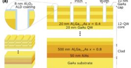
A Nanostructured Waveguide for Low-Density Polariton Condensation from a Bound State in the Continuum
August 2022
A Faster Way to Study 2D Materials for Next-Generation Quantum and Electronic Devices
August 2022
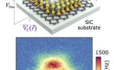
Autonomous Scanning Probe Microscopy Investigations of WS2 and Au{111}
May 2022
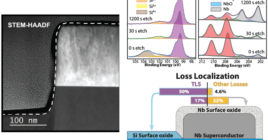
Localizing Sources of Quantum Decoherence
April 2022
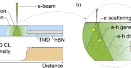
Optimizing Cathodoluminescence Spectroscopy Through Nanoscale Heterostructure Design
March 2022
An Electrical Trigger Fires Single Photons, One at a Time
October 2020
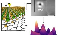
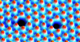
The Beauty of Imperfections: Linking Atomic Defects to 2D Materials’ Electronic Properties
November 2019
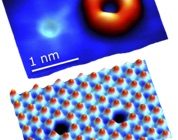
Linking Properties to Defects in 2D Materials
August 2019
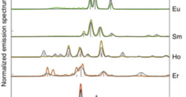
Multi-color Imaging with Sub-20-nm Cathodoluminescent Nanoprobes Using Electron Microscopy
March 2019
Berkeley Lab Highlights Molecular Foundry Intern in Lab Video Series
August 2017
New Properties Discovered in a 2-D Semiconductor
July 2017
Boosted Efficiency of Perovskite Solar Cells to 31 Percent
July 2016
Molecular Foundry Scientists Discover Surprising New Properties in a 2-D Semiconductor
May 2016
Precision Growth of Light-emitting Nanowires
February 2015
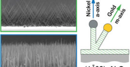
Switchable Control of Nanowire Growth
December 2014
Discovery of New Semiconductor Holds Promise for 2D Physics and Electronics
March 2014
Monolayer Behavior Retained in Bulk Semiconducting Transition Metal Dichalcogenide
March 2014
Cooling Microprocessors with Carbon Nanotubes
January 2014
Enhancing Thermal Transport of Carbon Nanotubes
December 2013
Foundry and NCEM Staff Gather to Identify Scientific Synergies
November 2013
Seeing in Color at the Nanoscale
March 2013
Was this page useful?
Send


