The Molecular Foundry hosted it’s annual NanoArt competition in celebration of National Nano Day – 10/9 – which helps raise awareness of nanotechnology, how it is currently used in products that enrich our daily lives, and the challenges and opportunities it holds for the future.
We had a number of great entries from the Molecular Foundry community, and now the votes are in! The top entries will be professionally printed and displayed in the Molecular Foundry’s lobby.
1st Place
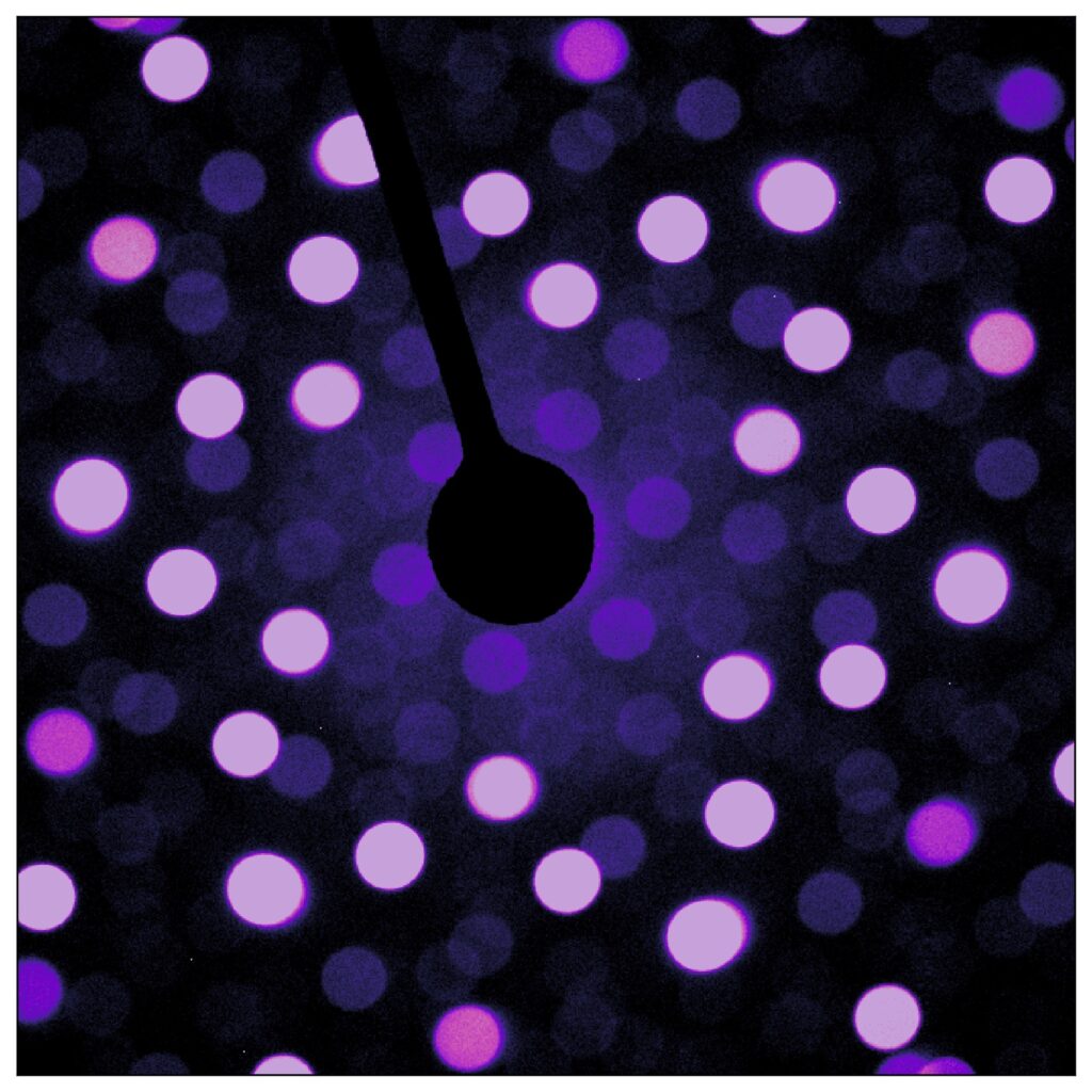
This image shows a converged beam electron diffraction pattern of a twisted bilayer of TaSe2, collected on the TEAM I microscope and submitted by Stephanie Ribet. Twisted bilayers of 2D materials are of great interest due to unusual physical, electronic, and optical properties that arise from the complex bilayer stacking. The features of interest in these materials are often on the nano scale, which makes electron microscopy imaging and diffraction an ideal tool to probe these structures. This TaSe2 stack forms a Moire pattern, which we can study with electron ptychography and interferometry.
2nd Place
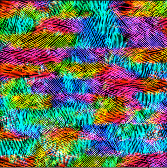
Submitted by Yael Tsarfati. An orientation map of a functional semiconducting polymer film, illustrating the polymer chains orientation. This map was derived from a 4D-STEM scan of a tilting sample in the TEAM I microscope. The samples was tilted from 0 to 20 degrees in steps of 2 degrees . The chains are colored based on their in-plane-projected orientations, visualizing the different crystalline domains. The polymer films are mixed conductors with a wide array of applications, spanning from energy storage, electrocatalysis, electrochromic devices, all the way to bio and neural sensing.
The image was created from work involving Yael Tsarfati, Karen Bustillio, and Colin Ophus.
3rd Place
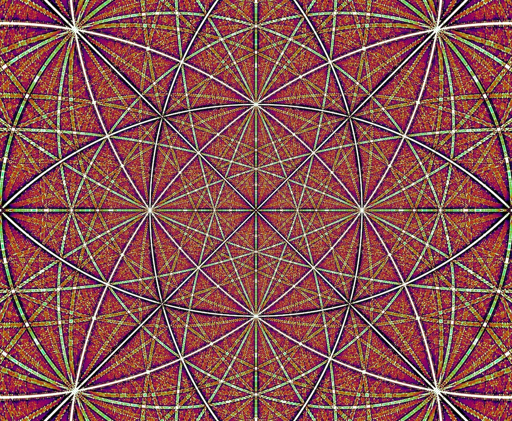
Submitted by Steven Zeltmann. The image is a simulation of the full Kikuchi map of a silicon crystal, shown in stereographic projection. The bands in the image correspond to particular symmetric directions of the crystal, and crystal is maximally symmetric at the locations where the bands cross. These patterns are used to determine the orientation of nanocrystalline materials and to aid in orienting single crystals for transmission electron microscopy.
4th Place
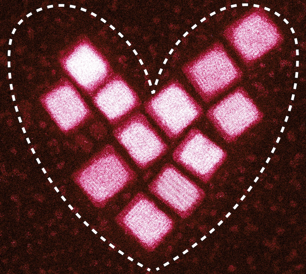
Submitted by Stephanie Ribet. This is a STEM image of core shell nanoparticles arranged in a heart. High resolution imaging with electron microscopy techniques can be used to establish structure-property relationships in nano materials. We investigated the structure of these core shell nanoparticles synthesized at the Foundry with STEM techniques on the TEAM 0.5 microscope.
5th Place
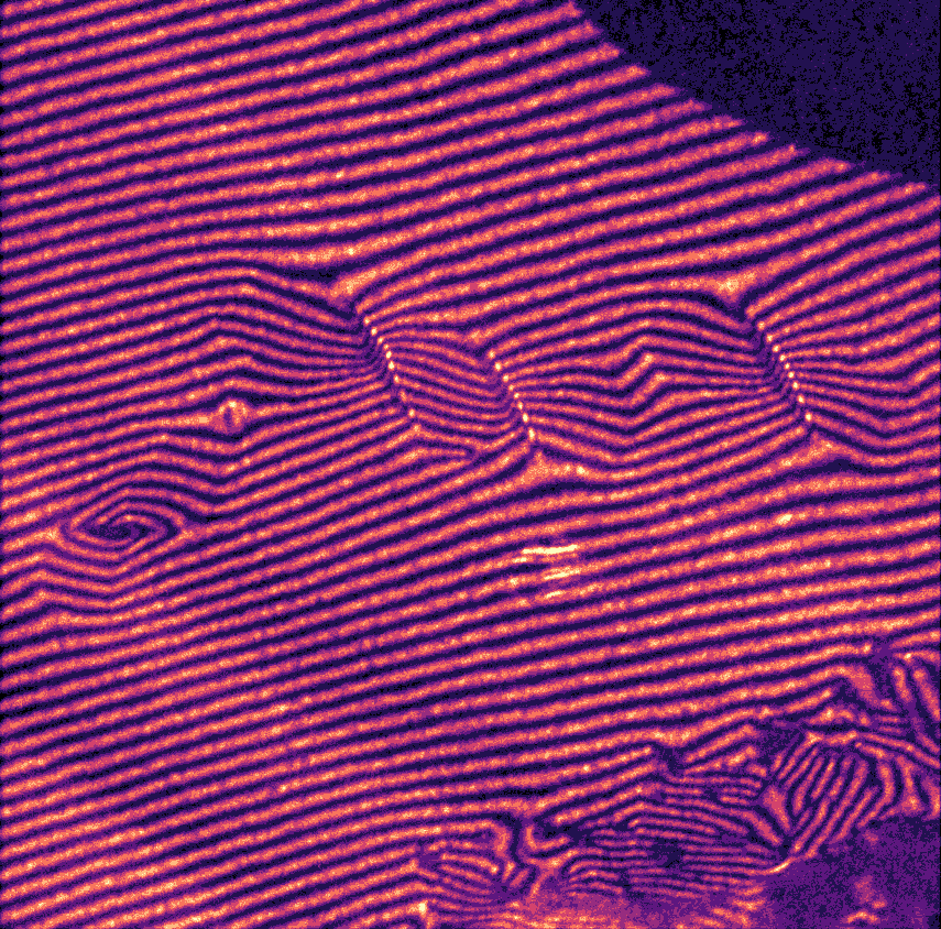
Submitted by Peter Schweizer. This is a Moiré interference pattern observed in a partially charged battery electrode. The features in the pattern are indicative of atomic scale defects and strain in the material. The observed phenomenon is important for the development of novel ion batteries.
6th Place
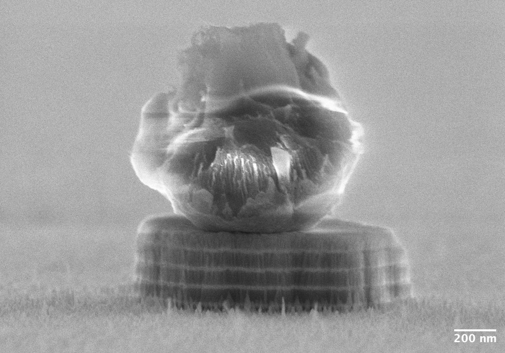
Submitted by Aidar Kemelbay. In celebration of the Nanoday, we prepared a Bragg cake with a polymer cherry on top. This structure was baked in oven at 650C in hydrogen disulfide to obtain transition metal dichalcogenide based all-dielectric Bragg reflector. Dielectric mirrors are important in many optics applications, such as microscopes, lasers, spectrometers and telescopes.
The work involved Aidar Kemelbay, Fabrizio Riminucci, and Marco D’Alessandro.
Honorable Mentions
