
During the summer, the Molecular Foundry supports several summer undergraduate students from UC Berkeley for a paid full-time summer internship (student benefits are the same as for the SULI program operated by LBNL). Transfer students are particularly encouraged to apply.
The internship program period spans 10 weeks from June 1, 2026 through August 7, 2026 and is administered by the Berkeley Lab Workforce Development and Education Office. Interns will participate in the same summer professional development programming as the SULI program. As an intern, participants will not only conduct research, but will participate in tours of Berkeley Lab facilities, lunchtime talks with researchers from across the lab, and more. The program culminates with a poster session where the interns present their research.
Continuing research opportunities after this time period may be available.
The deadline to apply for the summer 2026 program is February 1, 2026.
Eligibility:
- Must be a United States Citizen or Lawful Permanent Resident at the time of applying.
- Applicants must have an undergraduate cumulative minimum grade point average (GPA) of at least 3.0 on a 4.0 scale for all completed courses taken as a matriculated student at the applicant’s current (or recently graduated) institution and at any undergraduate institutions attended as a matriculated post-secondary student during the five years preceding the start of the current year.
- The FUSE internship is for rising juniors and seniors
- Interns cannot take classes while participating in the program.
Program Requirements:
The FUSE program is administered by the Berkeley Lab WDE office, which means that all FUSE interns will be required to complete all tasks associated with the SULI program.
- Complete the full 10-week program.
- Complete entrance and exit surveys.
- Make a poster presentation and submit a six- to eight-page research project report on the outcome of research activities.
- Attend all scheduled events, including lectures, tours, and group activities.
- Complete all Berkeley Lab safety and procedural requirements.
- Must behave in a responsible and professional manner. Interns must adhere to the Ethics and Conduct at Berkeley Lab Requirements and Policies Manual (RPM).
- Complete all assignments and deliverables including intern/mentor photos.
Application Information
The application for the 2026 FUSE program is now open with a deadline of February 1, 2026. If you have questions about the program or application, please contact us.
The application requires two short essays (uploaded as a PDF), college transcripts, and project preferences, as well as demographic data for administrative purposes. This guidance document provides information about the essays so that applicants can draft them before completing the form.
Opportunities for the 2026 Summer Program
Project listings, as available, will be posted below. Interested students are welcome and encouraged to reach out to the PIs to discuss their interest in a particular project, or to learn more about a project. (Note that there may be a few late additions to this project list.)
Electrochemical Characterization of Transport through Bacterial Microcompartment Shell Proteins
Principal Investigators: Paul Ashby
Other Mentors: Yaqing Wang, Timothy Chiang
In bacterial systems, chemical reactions are often organized within protein-based compartments rather than occurring freely in solution. Our group explores how biomimetic confinement controls molecular transport, reactivity, and catalysis at the nanoscale. By combining electrochemical methods with scanning probe microscopy, we measure local, nanoscale transport through protein-based systems, inspiring new approaches to catalysis, energy conversion, and synthetic biology.
Project Description:
Bacterial microcompartments (BMCs) are protein-based organelles that spatially confine enzymatic reactions and regulate molecular transport through selectively permeable protein shells. In this project, the intern will help develop a novel scanned probe based electrochemical technique that is three orders of magnitude more sensitive than current methods. The innovation involves a CMOS based current sensing amplifier with novel noise rejection circuitry that is embedded in the substrate. This new tool should be capable of probing transport behavior through individual BMC shell proteins at the nanoscale. We will work to build the tool and perform proof of principle measurements. Ultimately, we will link protein structure to functional transport behavior, advancing our understanding of how confinement influences catalysis in biomimetic systems.
Main project goal or research question to be addressed by the intern:
What is the ultimate sensitivity and resolution of the new electrochemical characterization technique? What is the transport behavior of the BMC shell proteins?
Intern’s role:
- Learning how to use the Atomic Force Microscope to generate nanoscale images of the morphological and electrochemical properties of BMC proteins.
- Prepare samples for proof of principle measurements.
- Prepare and characterize BMC shell protein samples for electrochemical measurements.
- Assisting in the collection, analysis, and interpretation of the electrochemical data
- Present the findings to the group or in a short written report
What can the intern expect to learn?
- How to use the Atomic Force Microscope.
- Protein assembly and deposition for sample preparation.
- Hands-on experience with transport measurements at the nanoscale.
- Skills in data analysis, scientific reasoning, and presentation.
- Interdisciplinary research bridging biology, chemistry, and electrical engineering.
AI-Driven Financial Data Visualization Agent
Principal Investigator: Ed Barnard
Other Mentors: Deirdre Olynick and Morgan Wall
This team is a collaboration between the Foundry’s Data Group and Finance team, combining Data Science and AI with applications in science and finance
Project Description:
Students will create an AI agent that takes user-input financial data (in formats like CSV or JSON), processes it, and generates graphs for visual analysis to support business operations. The AI agent will provide insights into financial trends and help users visualize key performance indicators (KPIs). Additionally, the project will be designed to be extendable for scientific data visualization, allowing students to apply their skills to various fields.
Main project goal or research question to be addressed by the intern:
Develop a version 1 AI agent for on demand data visualization
Intern’s role:
- Understand financial data formats and the significance of various financial metrics (e.g., revenue, expenses, profit margins).
- Learn how to process and analyze financial data using Python.
- Utilize data visualization libraries to graph financial data for business operations.
- Implement basic AI techniques to derive insights from financial trends.
- Build a simple user interface for interaction and future adaptation for scientific
What can the intern expect to learn?
- Relevance of financial data and visualization
- How to use and modify open source AI tools for data processing
- How AI agents will be relevant in finance and scientific research
Synthesis of High-Quality Non-Linear Optical Materials
Principal Investigator: Shaul Aloni
Other Mentor: Tevye Kuykendall
In the Inorganic Facility of the Molecular Foundry, we develop methods for gas-phase synthesis of nanostructures such as nanowires, nanotubes, and 2D films. Recently, we acquired a new Cluster Tool capable of thin film synthesis and characterization. For this project, we will focus on developing synthetic and characterization protocols for prototypical high performance nonlinear optic materials, such as lithium niobate.
Project Description:
With superconducting RF circuits emerging as a leading platform for quantum computing and optical photons being the most likely quantum information carrier, the integration of optical and microwave components is a crucial step in the development of scalable and efficient quantum computing architectures. Quantum transducers, which enable the controlled conversion of a signal or excitation from one physical carrier to another while preserving the information content, are essential to bridging this gap. Specifically, transducers that map a quantum state between microwave and optical bosonic modes via engineered interactions, aiming for phase-coherent conversion, are required. For this proposal we will focus on developing synthetic protocols for a prototypical high performance nonlinear optic material lithium niobate (LN). we will use a new materials exploration cluster tool capable of pulsed laser deposition (PLD), atomic layer deposition (ALD), and reactive sputtering. This versatile tool combines various deposition techniques with an automated transfer system and in-situ analytical tools, facilitating a highly controlled and optimized synthesis workflow.
Main project goal or research question to be addressed by the intern
The main goal is to explore and optimize different synthetic conditions for growing LN films. The synthesis portion of the project will study process conditions of PLD, ALD, or reactive sputtering, and focus on several characterization techniques, such as XRD, SEM and optical spectroscopy.
Intern’s role:
- The intern will learn how to conduct research on solid state materials synthesis.
- They will be responsible for synthesizing LN thin films using one or more techniques.
- They will learn how to characterize their samples using a variety of analytic techniques.
- They will learn how to interpret results, and make improvements to the synthetic process using feedback for successive experiments.
They will receive careful oversight over the course of the internship, working closely with a foundry postdoc on this project. They will be trained to independently operate analytical tools to characterize the LN films. Additional training will be given as needed. Regular discussions will be had to interpret results and gauge progress.
What can the intern expect to learn?
The intern will learn a variety of synthetic and analytic techniques, such as:
- Thin film deposition techniques, such as pulsed laser deposition, atomic layer deposition, and reactive sputtering.
- X-ray diffraction
- Optical spectroscopy
- Scanning electron microscopy
- They will be mentored in the creation of a final poster project and will learn how to present their data using written text, plots, photographic images, and illustrations.
Improving CO2 capture and conversion with a synthetic Rubisco aggregate
Principal Investigator: Crysten Blaby
We investigate how biological systems encode functionality across genomic architectures, protein assemblies, supramolecular complexes, and hierarchical bioproducts at the molecular to nanoscale. Using computational genomics approaches integrated with hypothesis-driven experimentation, we aim to define the foundational design principles and structure-function relationships needed to engineer bio-based nanomaterials, functional biointerfaces, and transformative biotechnologies that seed new economic opportunities.
Project Description:
The pyrenoid is a membrane-less, phase-separated organelle within chloroplasts, formed by the condensation of the CO2-fixing enzyme Rubisco, which is critical for global carbon assimilation. Its primary function is to locally increase CO2 concentration around Rubisco, compensating for the enzyme’s inefficiency in discriminating between CO2 and O2, with recent research highlighting the role of intrinsically disordered proteins as “molecular glue” in its liquid-liquid phase separation. Notably, Auxenochlorella protothecoides, an industrial alga being engineered for carbon-neutral jet fuel, lacks a pyrenoid, necessitating expensive high CO2 culture conditions for optimal growth. Therefore, reconstructing the pyrenoid in A. protothecoides could significantly enhance biomass accumulation, increase biomaterial production, improve CO2 assimilation, and provide fundamental insights into biological condensates for advanced carbon capture technologies.
Main goal of the project:
To identify and characterize candidate intrinsically disordered proteins (IDPs) involved in pyrenoid formation.
Intern’s role:
This project will involve bioinformatics to identify potential IDPs, and potentially microscopy to observe where they localize within A. protothecoides, providing foundational insight for future pyrenoid reconstruction efforts.
What can the intern expect to learn?
Bioinformatics and optical microscopy
Long-wavelength fluorescent antibody conjugates
Principal Investigator: Bruce Cohen
Other mentor: Isha Nadig
Optical microscopy is the primary means of studying complex living systems, enabling real-time analysis of individual cellular components at high spatial and temporal resolution. The Cohen lab develops novel optical probes as biosensors, improving bioconjugation and targeting chemistries, and imaging live systems with these reagents. We aim to integrate the development of novel luminescent nanomaterials into multidisciplinary efforts to address significant biological questions of cell function.
Project Description:
Labeling of antibodies with organic fluorophores is a cornerstone of bioimaging, but there are ongoing challenges with current antibody bioconjugation techniques. One problem is that many organic fluorophores are unstable under the reaction conditions needed to form stable fluorescent antibody conjugates. These include novel fluorophores that emit past 1000 nm, in the NIR-II range. We are developing a simple method for labeling clinically relevant IgG antibodies with fluorophores that are unstable under standard reaction conditions, and a goal of this internship is to contribute to the synthesis of these long-wavelength fluorophores.
Main research question
This project then entails synthesis of organic fluorophores in the NIR-II region, past 1000 nm.
Intern’s role:
The intern will learn and perform the basics of organic synthesis, chemical and optical characterization, and some bioconjugation chemistry. In addition to these techniques, the intern will learn about fluorescence, immunotargeting, the science of bioimaging, and how to prepare talks and papers.
What can the intern expect to learn?
See above!
Electronic Structure and Spectroscopy of Defect-Based Qubits in Nitride Semiconductors
Principal Investigator: David Prendergast
Other mentor: Adway Gupta
The research of the group is focused on modeling properties of nanostructure systems from first principles using a range of computational and data-driven techniques. Examples include simulating the X-Ray absorption and photoluminescence spectra of material systems to gain a better understanding of their electronic structure, predicting product synthesizability of coupled chemical reactions and modeling molecule conformers close to solid-liquid interfaces.
Project Description:
Modern quantum information technologies rely on quantum bits (qubits) that exhibit long coherence times and can be reliably synthesized and integrated into solid-state platforms. Group-13 nitrides (BN, AlN, GaN, and InN) are promising host materials for such qubits due to their wide bandgaps, the presence of deep defect states, and well-established growth and fabrication techniques, which together can isolate qubit energy levels from the surrounding electronic continuum. However, atomic rearrangements and lattice relaxations in the vicinity of defect sites can significantly alter defect stability and electronic structure, meaning that not all defects are viable or possess the energy landscape required for robust qubit operation. A systematic exploration of the defect phase space is therefore essential to identify stable, optically addressable defects suitable for quantum information applications.
Main project goal or research question to be addressed by the intern
The goal of this project is to identify defects (vacancies, substitutions, complexes) in group 13 nitrides that can act as functional qubits, by determining their formation energies, energy ordering, and X-Ray absorption spectra from first principles.
Intern’s role:
The intern will construct and analyze a range of point-defect configurations in group-13 nitride materials (M–N, with M = B, Al, Ga, In). They will perform structural relaxations to determine defect-induced atomic rearrangements and identify the lowest-energy configurations, followed by calculations of defect formation energies. Using advanced electronic-structure methods, the intern will then determine the energy level ordering of these defects and assess their suitability for qubit applications. Finally, the intern will map the electronic structure to simulated X-ray absorption spectra, which can support and guide experimental efforts into the characterization of such systems.
What can the intern expect to learn?
Through this project, the intern will gain hands-on experience with Density Functional Theory (DFT) and learn how it is used to study the electronic structure of real materials. They will also be introduced to more advanced approaches built on DFT, such as constrained DFT, Koopmans-compliant functionals, and hybrid functionals, and understand when and why these methods are needed. In addition, the intern will learn how to run and manage large-scale, parallel simulations on modern high-performance computing systems. Furthermore, they will develop a strong foundation in condensed matter physics, electronic structure theory, and light–matter interactions, as well as practical skills in analyzing and interpreting computational results.
Crystal Engineering of Polymeric Structures with Dative Boron–Nitrogen Bonds
Principal Investigator: Jian Zhang
The Zhang group at the Foundry investigates the synthesis and emerging properties of self-assembly of molecular building blocks. The resulting close-packed molecular crystals or porous framework materials exhibit tunable chemical, physical, optical, or mechanical properties for potential energy-related applications. This requires a deep understanding of the structure-property relationship across spatial and temporal scales, particularly through the use of dynamic covalent chemistries.
Project Description:
Crystalline porous materials, such as Metal-Organic Frameworks (MOFs) and Covalent Organic Frameworks (COFs), are widely used for catalysis and separation. However, a developing class of materials based on dative boron-nitrogen (B-N) bonds offers a unique “middle ground” between strong covalent bonds and weaker non-covalent interactions. These B-N bonds (N ®B) are isoelectronic to C-C bonds but possess dynamic reversibility, allowing for error correction during crystallization and the formation of defect-free single crystals.
Despite their potential, constructing robust, high-dimensional (2D or 3D) polymeric structures using B-N bonds remains a significant challenge. The inherent flexibility and reversibility often lead to the formation of discrete molecular cages or low-dimensional macrocycles rather than the desired extended networks. Furthermore, predicting the final crystal structure is difficult due to the specific conformational preferences of Lewis acid-base adducts, such as the tendency for pyridyl rings to orient orthogonally to boronate esters.
Main project goal or research question to be addressed by the intern
The main goal of this project is to apply advanced crystal engineering strategies to overcome these limitations and synthesize robust, single-crystalline B-N polymeric frameworks. We will investigate novel design strategies, including:
- Electrostatic Complementarity: Utilizing electron-deficient and electron-rich aromatic centers to stabilize 3D networks with high connectivity, similar to the “sandwich nodes” observed in recent robust frameworks.
- Synergistic Assembly: Combining B-N bonds with other interactions, such as halogen bonds, to direct the self-assembly of 2D nanoribbons or sheets.
- Adaptisorption Mechanisms: Designing nonporous crystals that can dynamically undergo “dissolution-adsorption-recrystallization” to capture guest molecules, a phenomenon recently defined as adaptisorption.
This research aims to expand the toolbox of reticular chemistry by establishing design rules for B-N polymers that combine the crystallinity of MOFs with the light-weight nature of organic polymers.
Intern’s role:
- Synthesis of Monomers: Synthesize and purify rationally designed polytopic Lewis acid ligands (e.g., boronate esters) and Lewis base linkers (e.g., pyridyl-based cores).
- Crystal Growth Optimization: Explore solvothermal and slow-cooling crystallization conditions to balance the thermodynamics and kinetics of B-N bond formation, aiming for large, single crystals suitable for X-ray analysis.
- Structural Characterization: Determine the crystal structures of the resulting polymers using single-crystal X-ray diffraction (XRD). The intern will analyze topological features, such as “Luban Lock” configurations or helical chains, to understand packing modes.
- Property Investigation: Test the stability of the frameworks in various solvents and temperatures, and investigate their dynamic properties, such as guest-induced structural transformations (adaptisorption) or photocatalytic activity.
What can the intern expect to learn?
- Hands-on experience in organic synthesis and the principles of dynamic covalent chemistry and supramolecular assembly.
- Advanced Crystallography: Deep understanding of single-crystal X-ray diffraction techniques, including data collection, structure solution, and refinement of complex polymeric structures.
- Reticular Chemistry Design: How to use crystal engineering concepts (topology, node connectivity, non-covalent interactions) to design functional materials.
- Scientific Communication: Skills for presenting complex structural data and mechanisms via interactions with the PI, group meetings, and poster sessions.
Fabricating high resolution DNA arrays for high-throughput datasets of protein-DNA complexes
Principal Investigator: Behzad Rad
Other mentors: Selven Virasawmy
We use fabrication and single molecule microscopy to visualize nanoscale and biological materials with high precision. Learning how these systems assemble and function, we can use this knowledge to engineer new complex structures for application in materials synthesis and catalysis.
Project Description:
DNA binding proteins serve essential functions in the cell from genome maintain to high fidelity DNA repair, replication and translation. These proteins have also led to the development of breakthrough therapeutics, e.g. CRISPR based gene therapy, as well as the design of high-end devices for DNA sequencing and detection of pathogens. Understanding the mechanism of protein-DNA complexes is key first step to designing new proteins with custom function. To do so, a large data set of biochemical and functional assays are required to develop new AI models linking protein design to function.
DNA arrays have been a powerful tool for visualizing and understating protein-DNA interactions. These molecular arrays allow for direct measurement of hundreds of proteins in parallel on DNA. Current methods of constructing DNA arrays are expensive, requiring repeated fabrication of nanostructures on glass substrates. To design a new, reusable system for construction of DNA arrays, we plan to use negative template to pattern proteins, which in turn will allow DNA to be arrayed onto modified glass substrates with a specific spacing. The construction will allow the fabrication of DNA arrays to allow for direct visualization of 50 to 100 protein-DNA complexes in parallel, creating large datasets for protein function. These datasets will enable mechanistic understanding of these systems as well as build up training data for training AI models to link protein structure and design to function on DNA.
Main project goal or research question to be addressed by the intern:
We plan to create a fabricated DNA arrays using a nanostructured silicon template, which can then be used to visualize protein-DNA at the single molecule level. We will use fabricated arrays as reliefs to create defined protein patterns for transfer onto modified glass substrates. We will then measure and test these protein patterns for the ability to array DNA using high resolution microscopy. These experiments will then inform the optimal dimensions and conditions for creating reproducible protein arrays down to 100 nanometers.
Intern’s role:
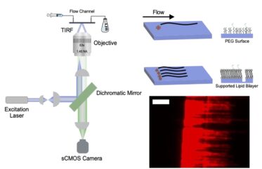
The internship will involve bench top fabrication, surface chemistry, bioconjugation, Atomic Force and Fluorescence Microscopy to acquire images of protein and DNA arrays, respectively. Data analysis of image stacks will also be needed to measure single molecule DNA arrays.
What can the intern expect to learn?
The intern should expect to learn bioconjugation techniques for DNA, fabrication processes and methods, high resolution imaging using state of the are microscopes, and image analysis methods.
Real- time, Quantitative Probe and Surface Reconstruction in Atomic Force Microscopy
Principal Investigator: Thomas Darlington
Other Mentors: Paul Ashby, Alex Weber-Bargioni
This team focuses on high-resolution structural and electronic imaging of hard and soft matter systems.
Project Description:
The main goal is to develop a computational pipeline to reconstruct the structural morphology of scanning probe microscopy (SPM), particularly atomic force microscopy (AFM), from in situ SPM datasets using AI/Machine Learning approaches, especially physics informed models. Accurate estimate of the probe shape will enable more quantitative and repeatable structural and electrical characterizations which is crucial for high throughput SPM experiments. Initially, project will focus on AFM in air, but will eventually include advanced techniques SPM such as non-contact AFM in ultra-high vacuum, as well as field-based techniques such as Kelvin-probe force microscopy and scanning near-field optical microscopy. Ultimate goal is to develop an autonomous agent that can analyze SPM data real time and provide reasonable information on the probe.
Main project goal or research question to be addressed by the intern:
To develop a computational pipeline to reconstruct the structural morphology of scanning probe microscopy (SPM), particularly atomic force microscopy (AFM), from in situ SPM datasets using AI/Machine Learning approaches, especially physics informed models. Accurate estimate of the probe shape will enable more quantitative and repeatable structural and electrical characterizations which is crucial for high throughput SPM experiments. Initially, project will focus on AFM in air, but will eventually include advanced techniques SPM such as non-contact AFM in ultra-high vacuum, as well as field-based techniques such as Kelvin-probe force microscopy and scanning near-field optical microscopy. Ultimate goal is to develop an autonomous agent that can analyze SPM data real time and provide reasonable information on the probe.
Intern’s role:
Using python based coding, intern will principally be performing advanced image analysis on SPM datasets, including AI/ML tools. Intern will also participate in SPM experiments, with support of the mentor, acquiring needed training datasets, and ultimately deploy developed computation tools via integration with the ScopeFoundry platform.
What can the intern expect to learn?
The project will allow the intern to learn fundamental image analysis techniques, such as image deconvolution, image registration and alignment, and Fourier Analysis, as well as advanced topics such as physics-based machine learning. Intern will also have the opportunity to gain hands-on experience with research imaging tools such as AFM, scanning electron microscopes, and optical microscopes.
Design and Application of Digital Microfluidic Platforms for Biological Assays
Principal Investigator: Aeron Tynes Hammack
Other Mentor: Harika Dechiraju
The Tynes Hammack group focuses on developing single-particle sensing devices to better understand self-assembly processes in single and multicellular life. By creating nanofluidic integrated circuits and digital microfluidic devices, we aim to enable precise optical and electrical analysis of nanoparticles and biological materials. This approach bridges nanofabrication and biological nanostructures to unlock transformative insights in microbiology and molecular biology.
Project Description:
This project aims to develop and apply digital microfluidic (DMF) devices to miniaturize conventional biological assays for studying host–pathogen interactions between bacteria and bacteriophages. By combining hands-on wet lab techniques with cutting-edge microfluidic technology, the project enables high-precision, small-volume experiments that allow individual bacterial–virus interactions to be examined at scale. Using DMF platforms, the research will investigate bacterial and phage behavior, genetic and protein-level responses, and metabolic activity. The project also explores the broader development of DMF devices, including optimizing design of electrodes and materials for improved device performance.
Main project goal or research question to be addressed by the intern:
How can digital microfluidic platforms be used to miniaturize biological assays and improve precision in studying host–pathogen interactions?
Intern’s role (i.e., what kinds of things will they be doing):
- Assist in testing and optimizing digital microfluidic devices for bacterial and bacteriophage assays
Perform wet lab experiments, including bacterial and phage culture, PCR, and long-read sequencing
Participate in optical and fluorescence imaging and spectroscopic characterization
Conduct an independent research project under the guidance of postdoctoral researchers and the faculty mentor.
What can the intern expect to learn?:
- Hands-on operation of digital microfluidic systems for biological experiments
- Core laboratory techniques such as microbial culture, DNA/RNA handling, sequencing, and microscopy
- How to design, execute, and analyze a scientific research project
- Scientific communication and presentation skills through group meetings, discussions with researchers, and a final poster presentation
Automated Fabrication and Optimization of 2D Material Heterostructures
Principal Investigator: Archana Raja
Other Mentors: Laisi Chen, Aadhish Ramanathan
The research group focuses on fabrication and optical characterization of low dimensional materials, and incorporating automation and AI technology to optimize research efficiency and outcome.
Project Description:
This project seeks to develop an automated platform for the precise fabrication of 2D material heterostructures. By integrating robotics with reinforcement learning, a motorized 2D materials transfer system and robotic arm is trained to assemble high-quality heterostructures within an inert atmosphere, minimizing the need for human intervention. Leveraging an agentic AI framework, the system can fabricate diverse heterostructure stacks while dynamically optimizing key variables based on reinforcement learning and insights from the literature. The ultimate objective is to achieve reproducible, high-quality sample fabrication with a success rate and structural precision surpassing that of conventional manual methods.
Main project goal or research question to be addressed by the intern:
Developing the completed automated stacking process to create an intended 2D materials heterostructure.
Intern’s role (i.e., what kinds of things will they be doing):
Collecting sufficient training data of the transfer process from various materials and conditions. Updating the design of the supporting structures for better performance.
What can the intern expect to learn?
AI/ML, data collection, data management, robotics, nanofabrication of 2D materials.
Merging lead-halide perovskites with quantum metaphotonics : achieving few-to-single photon super-radiance and exploring their resonantly-boosted quantum photo-physics.
Principal Investigator: Archana Raja
Other Mentors: Mashnoon Alam Sakib, Dr. Laisi Chen, Kang’an Wang, Misael Campos
The research group has expertise in imaging, fabrication and manipulation of nanostructures. We regularly perform low-temperature cryogenic spectroscopy and time-resolved dynamics of quantum-dot like photon emitters.
Project description
Organic-inorganic lead-halide perovskite nanocrystals (LHP NCs) hold the promise for next-generation semiconductor materials with their robust quantum optoelectronic properties along with superior manufacturability1. The inherent construction of these LHP NCs has been found to be mediated by ligand species, which plays a role in enhancing the quantum-photophysical properties such as photoluminescence quantum yield (PLQY) and optical stability for their mass-application in quantum-optoelectronic devices2,3. However, developing a controlled route to specifically tap onto the of quantum-electrodynamics of these LHP NCs have been less explored due to their intricate dependencies on their physical dimensions and growth3,4. This hindered accessing illusive quantum few-photon to single-photon nonlinear regimes which require more robust cavity-mediated interactions5. Artificially designed surfaces, also known as metasurfaces (MS), provide a pathway to design and implement specific ‘meta’-cavities that could be directly taken advantage to resonantly boost the cavity-electrodynamic processes4,5. Merging of such metaphotonic cavities with LHP NC-like quantum dots has still been less explored 5,6,7. In this project, we aim to develop a first-of-its’ kind artificial super-hybridized metaphotonic platform to specifically boost the quantum-nonlinearities of these LHP NCs by hybridizing them with specifically designed dielectric metasurfaces. The QMSs would enable a spatial and spectral overlap of the LHP NCs optoelectronic properties, allowing us to reach a super-radiance phenomenon along with tapping chiral-dependent emission characteristics that could lead to having few-photon to single-photon emission allowing their massive applications from a variety of use cases from photovoltaics, quantum photon sources for quantum cryptography and quantum information sciences.
References:
[1] Atomically resolved edges and defects in lead halide perovskites, Nature, volume 647, pages364–368 (2025)
[2] Constructing Lead Halide Perovskite Nanocrystal Surfaces, ACS Energy Lett. 10, 9, 4158–4183 (2025)
[3] Lead halide perovskites: Crystal-liquid duality, phonon glass electron crystals, and large polaron formation. Science Advances 3,e1701469 (2017).
[4] Opportunities and Challenges of Solid-State Quantum Nonlinear Optics, arXiv:2411.06630v1 [physics.optics] 10 Nov (2024)
[5] Free space few-photon nonlinearity in critically coupled polaritonic metasurfaces, Nature Communications, volume 16, Article number: 10099 (2025)
[6] Single-photon superradiance in individual caesium lead halide quantum dots, Nature, volume 626, pages535–541 (2024)
[7] Single-Photon Superradiance from a Quantum Dot, Physical Review Letters 116, 163604 – Published 21 April, (2016)
Main project goal or research question to be addressed by the intern
Engineer artificially-boosted quantum electrodynamic pathways for hybridized quantum dots.
Intern’s role
The intern will get hands-on experience on characterization and modeling of optical metasurfaces and characterization techniques
What can the intern expect to learn?
Design and characterization of metasurfaces, stewardship in optical spectroscopy characterization, data analysis, and modeling.
Thermodynamic computing in and out of equilibrium
PI Name: Stephen Whitelam
My group uses statistical mechanics and machine learning to study nanoscale dynamics and phenomena, including molecular-self assembly, driven nanoscale devices, and unconventional types of computing.
Project Description:
In classical computing, the energy scales of even the smallest devices, such as transistors and gates, are large compared to that of the thermal energy, k_B T. As a result, there is a clear separation of scales between signal and noise, enabling deterministic computation. This determinism comes with an energy cost: classical computers operate far above the limits of thermodynamic efficiency, and require large amounts of power and heat dissipation to ensure their reliability.
As devices shrink to the nanoscale, the energy associated with computation becomes comparable to that of thermal fluctuations, making computation more energy efficient. On these scales, thermodynamic computing makes use of the tendency of physical systems to evolve toward thermal equilibrium to do computation. The thermal bath contributes to computation by providing the fluctuations necessary for state changes, and in some modes of operation the signal the noise, with the equilibrium fluctuations of the degrees of freedom of the thermodynamic computer being the output of the calculation.
This project will involve the exploration of a classical digital computer model of a thermodynamic computer.
Main project goal or research question to be addressed by the intern:
To become familiar with the notion of thermodynamic computing, and to choose a direction in this field to explore. Thermodynamic computing is a new field, and there’s lots to explore! [Look up “Normal Computing” and “Extropic” to get an idea of what two startups in this field are working on]. The point of departure for this project could be this paper: https://arxiv.org/abs/2506.15121
Intern’s role (i.e., what kinds of things will they be doing):
Numerical simulations of physical systems, statistical mechanics, machine learning, learning to identify interesting research questions.
What can the intern expect to learn?
See above!

