Scientific Achievement
Researchers used dielectric probes to visualize and reversibly tune exciton emission inside nanoscale bubbles in WSe₂ monolayers by precisely controlling strain.
Significance and Impact
This provides a non-destructive method to create tunable single-photon sources from 2D materials, which could enable quantum communication devices and advanced optical sensors that can be precisely adjusted at the nanoscale.
Research Details
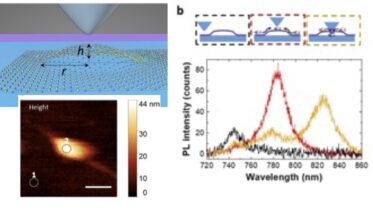
- The researchers used hyperspectral photoluminescence (PL) mapping to resolve the spatial and spectral emission profiles of strain-induced excitonic states, identifying a centralized wavelength distribution around 782 nm.
- Applying tip-induced strain enabled deterministic, reversible, and linear tuning of excitonic emission wavelengths, with shifts of up to 90 nm (≈180 meV) from the unstrained exciton wavelength (energy).
Zhou, J., Thomas, J.C., Darlington, T.P., Barnard, E.S., Taguchi, A., Schwartzberg, A., Weber-Bargioni, A. Advanced Materials. e03134 (2025) DOI: 10.1002/adma.202503134
Research Summary
This study demonstrates a method to control light emission from atomically thin materials using naturally occurring nanoscale bubbles in monolayer WSe₂. These bubbles form during fabrication and create localized strain that traps excitons—bound electron-hole pairs that emit light. Using dielectric near-field probes, the researchers mapped the emission properties within individual bubbles and found they emit at wavelengths centered around 780 nm. By applying controlled pressure with the probe tip, they achieved reversible tuning of the emission wavelength over a 50 nm range, with total shifts up to 90 nm from the unstrained material. Analysis of 67 bubbles revealed consistent emission characteristics, while power-dependent measurements showed that strain creates regions that concentrate light-emitting carriers at the nanoscale.
This work addresses practical challenges in developing tunable single-photon sources, which are needed for quantum communication and photonic devices. Unlike conventional approaches that create static strain patterns, this technique offers dynamic and reversible control over light emission. The non-destructive nature of the dielectric probe method, combined with the predictable behavior of these strain-engineered bubbles, provides a practical approach for controlling optical properties in 2D materials. This could be useful for applications in quantum information processing, optical sensing, and related photonic technologies where precise control of light emission at the nanoscale is required.

